XGB Analog edition manual
8.11 Configuration and Function of Internal Memory
An analog input option board has internal memory for data communication with XGB base unit.
8.11.1 Analog Data I/O Area
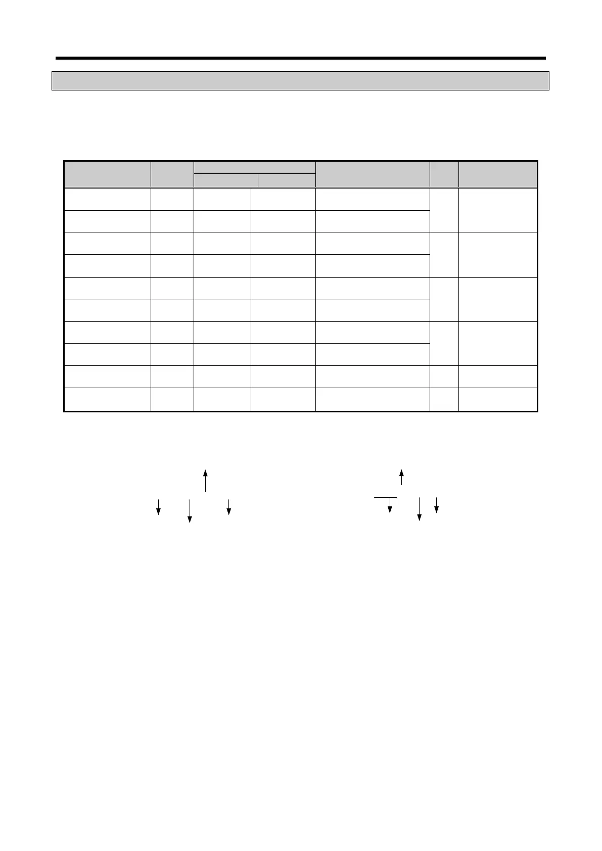
The table below presents the analog data I/O area.
Variable Type
Description
R/W
_0y_ERR BIT U0y.00.0 %UX0.y.0
Module Error
R
Option → CPU
_0y_RDY BIT U0y.00.F %UX0.y.15
Module Ready
_0y_AD0_ACT BIT U0y.01.0 %UX0.y.16
CH0 Active
R
Option → CPU
_0y_AD1_ACT BIT U0y.01.1 %UX0.y.17
CH1 Active
_0y_AD0_IDD BIT U0y.01.4 %UX0.y.20
CH0 Disconnection flag
R
Option → CPU
_0y_AD1_IDD BIT U0y.01.5 %UX0.y.21 CH1 Disconnection flag
_0y_AD0_ERR BIT U0y.01.8 %UX0.y.24
CH0 error
R
Option → CPU
_0y_AD1_ERR BIT U0y.01.9 %UX0.y.25
CH1 error
_0y_AD0_DATA WORD U0y.04 %UW0.y.4
CH0 Output
R
Option → CPU
_0y_AD1_DATA WORD U0y.05 %UW0.y.5
CH1 Output
R
Option → CPU
- In the device allocation, the small letter ‘y’ is the No. of the slot where the module is installed.
- For example, to read the ‘CH0 Input A/D Value’ of the analog module installed in the slot 9, write in
U09.05. (%UW0.9.4 for IEC types)
U 0 9 . 0 4
.
[ype]
.
[]
4
8 - 26