5.11.3.4 Allow All Message Classes to Print
1. At the MCC, type and enter: CHG:LPS,MSGCLS=ALL,PRINT=ON,LOG=ON;
Response: OK (with exception)
5.11.3.5 Inhibit Brevity Control
Caution: Brevity control should not be inhibited for more than ten switching
modules, concurrently. This can cause the loss of receive-only printer (ROP)
messages.
1. At the MCC, either:
type and enter: INH:BREVC,SM=a;
or
type and enter: 609 (1800,a CMD)
Where: a = Switching module number.
Response: OK
5.11.4 SAFE STOP POINT
1. This is a Safe Stop Point.
5.11.5 VERIFY TIMING REFERENCE CONNECTIONS
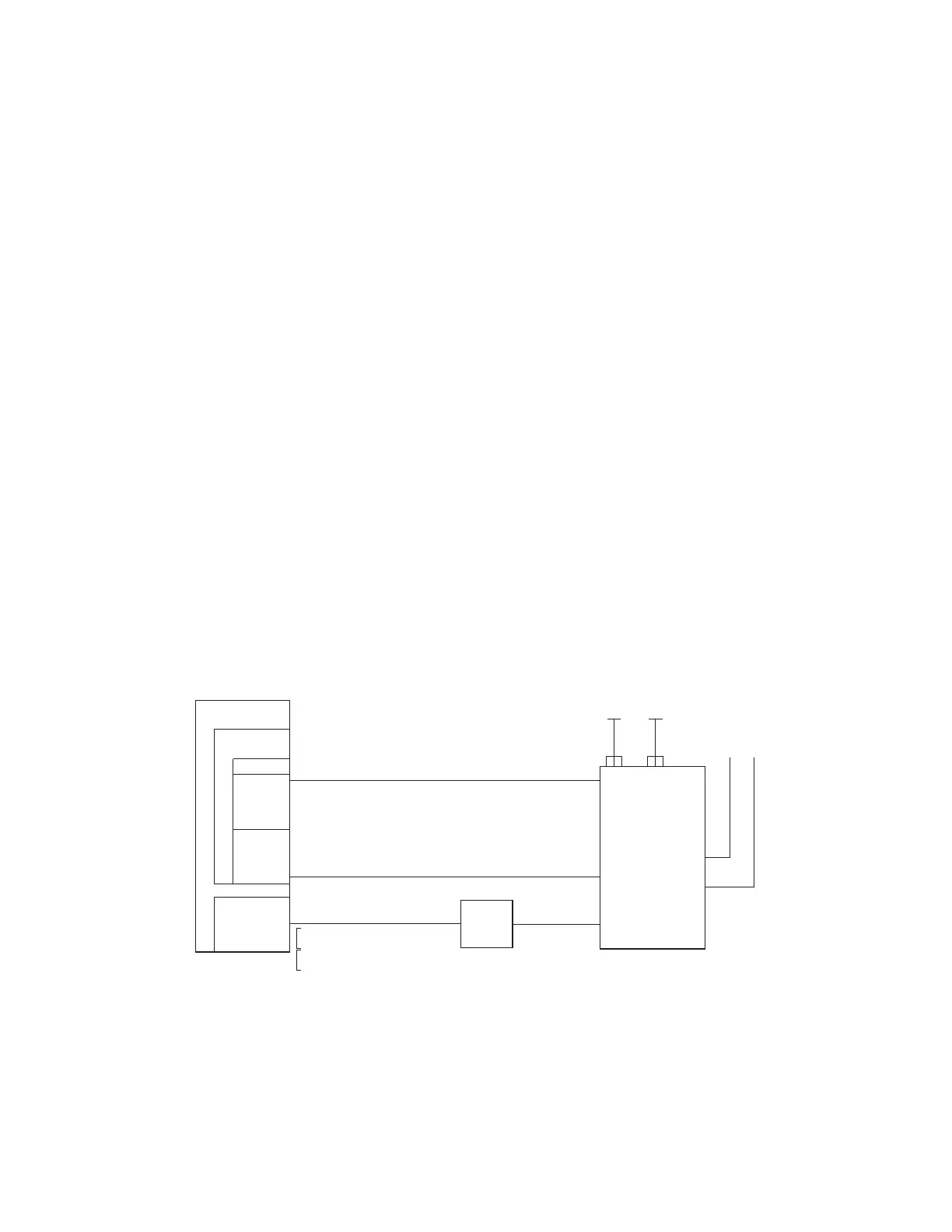
1. Verify that timing reference cables are installed (see Figure 5.11-1):
• Input clock reference cables to BITS box.
• Output clock reference cables between BITS box and TSIU4/TSIU4-2.
2. At the MCC Page 1190, verify that both Module Controller/Time Slot Interchange
(MCTSI) 0 and 1 are ACT/STBY.
TSICOM
SIDE 0
TSICOM
SIDE 1
UM74D
MMSU
MCTSI
TSIU4
SM-2000
ED5D765-11,G14 (EMC)
MMSU SCAN POINTS
MDF
ED5D765-11,G11
ALARMS
ED5D500-21,G104 & G105 (SWC)
ED5D503-30,G53 & G54
ED5D500-21,G104A & G105A (711)
ED5D503-30,G53A & G54A
ED5D500-21,G104B & G105B (TRW)
ED5D503-30,G53B & G54B
OUTPUT CLOCK REF SIDE 1
OUTPUT CLOCK REF SIDE 0
(SAME AS SIDE 0)
-48V POWER CABLE
ED5D765-11, G18
BITS
BOX
INPUT
CLOCK
REFs
TO
MMFU
Figure 5.11-1 — BITS BOX Cabling
235-200-150
January 2003
ROUTINE MAINTENANCE
Procedure 5.11
Issue 3.00 Page 5.11-3