26
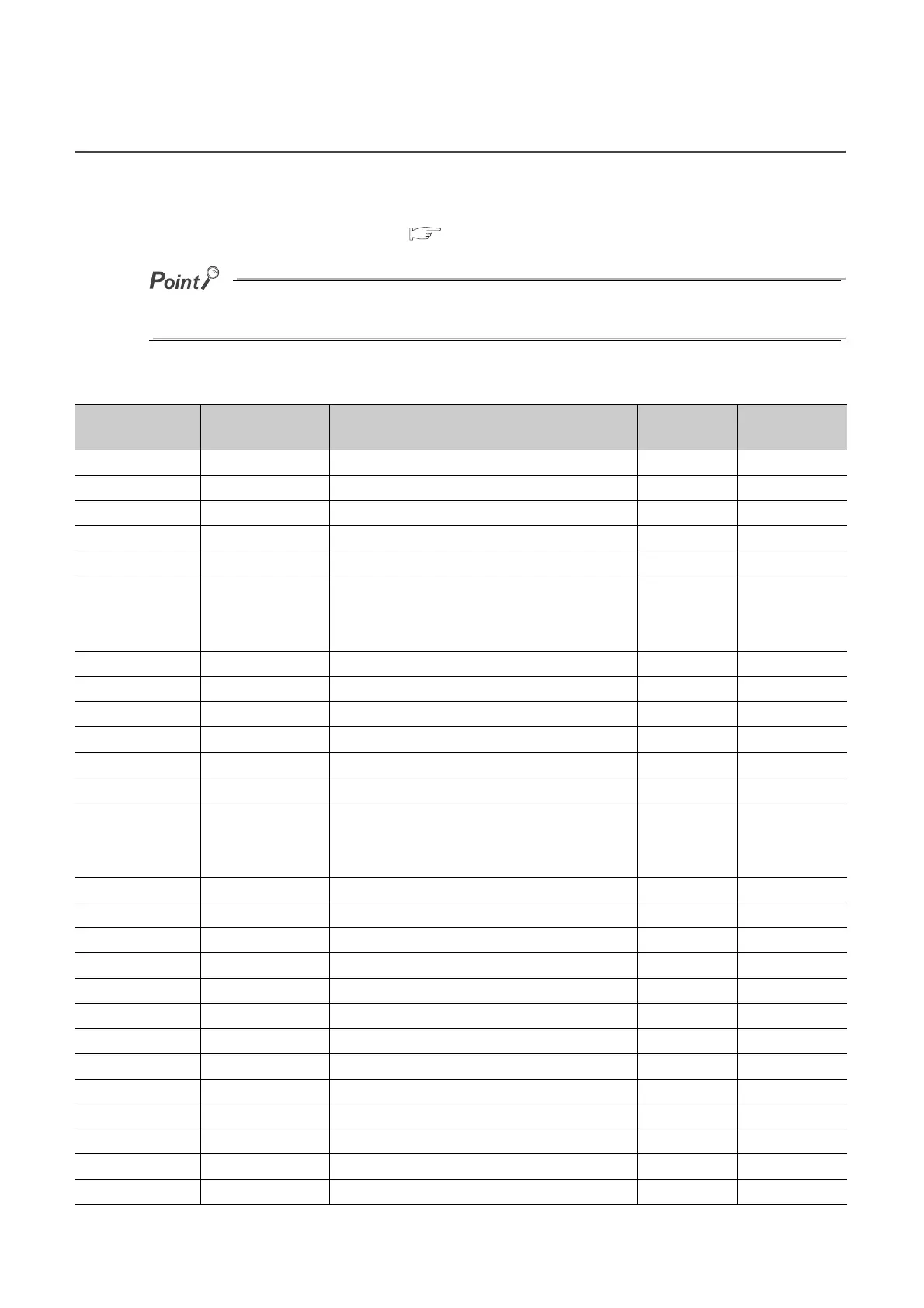
3.5 List of Buffer Memory Addresses
The following shows the list of the A/D converter module buffer memory.
For details of buffer memory addresses, refer to the following.
• Details of buffer memory addresses ( Page 174, Appendix 2)
Do not write data to the system area and the area where the data cannot be written from the program in the buffer memory.
Writing data to these areas may lead the module to malfunction.
(1) Un\G0 to Un\G1799
Address
(decimal)
Address
(hexadecimal)
Name
Default
*1
Read/Write
*2
0
0
H
A/D conversion enable/disable setting
0000
H
R/W
1
1
H
CH1 Time Average/ Count Average/Moving Average 0 R/W
2
2
H
CH2 Time Average/ Count Average/Moving Average 0 R/W
3
3
H
CH3 Time Average/ Count Average/Moving Average 0 R/W
4
4
H
CH4 Time Average/ Count Average/Moving Average 0 R/W
5
5
H
System area ⎯⎯to to
8
8
H
9
9
H
Averaging process setting (used to replace Q64AD)
0000
H
R/W
10
A
H
A/D conversion completed flag
0000
H
R
11
B
H
CH1 Digital output value 0 R
12
C
H
CH2 Digital output value 0 R
13
D
H
CH3 Digital output value 0 R
14
E
H
CH4 Digital output value 0 R
15
F
H
System area ⎯⎯to to
18
12
H
19
13
H
Latest error code 0 R
20
14
H
Setting range
0000
H
R
21
15
H
System area - -
22
16
H
Offset/gain setting mode Offset specification
0000
H
R/W
23
17
H
Offset/gain setting mode Gain specification
0000
H
R/W
24
18
H
Averaging process setting
0000
H
R/W
25
19
H
System area ⎯⎯
26
1A
H
Conversion speed setting
0001
H
R/W
27
1B
H
Input signal error detection extension setting
0000
H
R/W
28
1C
H
System area ⎯⎯
29
1D
H
Digital clipping enable/disable setting
000F
H
R/W
30
1E
H
CH1 Maximum value 0 R
31
1F
H
CH1 Minimum value 0 R
 Loading...