Home
Neoway
Control Unit
N75
Page 12 (Block Diagram)
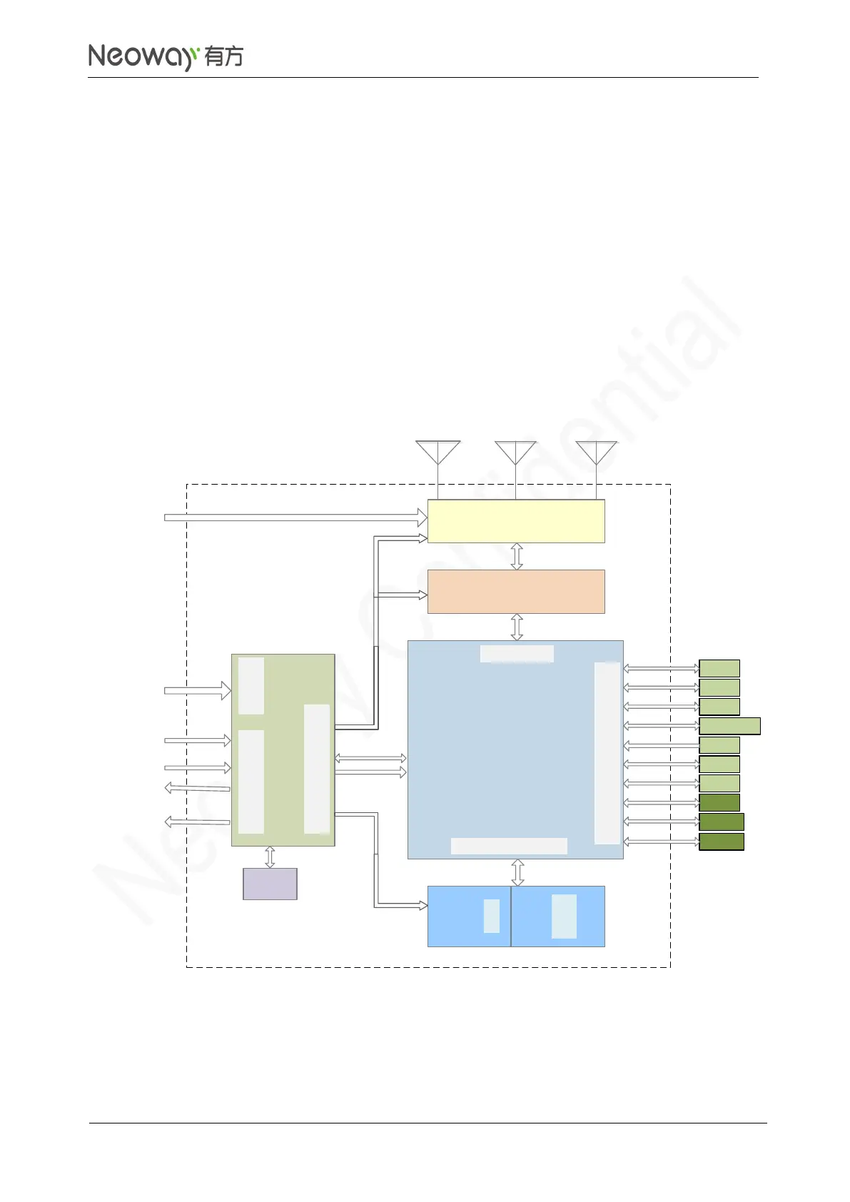
Neoway N75 - Block Diagram; Figure 1-1 Block Diagram
95 pages
Manual
Save Page as PDF
To Next Page
To Next Page
To Previous Page
To Previous Page
Loading...
N75
Hardware
User
Guide
Copyright © Neoway
T
echnology Co., Ltd
2
1.2
Block Diagram
N75 consists of the following functionality units:
⚫
Baseband
⚫
MCP
⚫
Power management unit
⚫
19.2MHz crystal oscillator
⚫
RF section
⚫
Digital interfaces (USIM, SPI, I2C, SGMII, SDIO,
ADC, GPIO, UART
, USB)
Fi
gu
re
1
-1
B
lo
ck
D
ia
gr
am
VBAT
RF tra
nscei
ve
r
19
.2
M
c
rysta
l
R
F
F
ront-
end
(
PA
/ASW/DUP/SAW)
AN
T
_
MA
IN
AN
T
_D
I
V
AN
T_GNS
S
PWRKEY
R
E
SE
T
MCP
NAND
LPDD
R
2
SDRA
M
B
a
s
e
B
and
MEM
OR
Y
S
UPPOR
T
R
FFE
I/F
S
C
ON
NEC
TI
V
I
TY
SP
MI
VDDs
TR
X
TR
X&MIP
I
Inp
ut
PM
Ou
tput
PM
Int
er
f
a
c
e
s
ADC
PM
_GPI
Os
VBAT
U
A
RT
SPI
I2C
AD
C
U
S
B
SGMI
I
SD
I
O
U
IM
GPI
O
I2S
/P
C
M
Power
Manager
VDDs
for
MCP
VDDs
for
P
A
/
ASW
11
13
Table of Contents
Main Page
Default Chapter
3
Table of Contents
3
1 About N75
11
Product Overview
11
Table 1-1 Variant and Frequency Bands
11
Block Diagram
12
Figure 1-1 Block Diagram
12
Basic Features
13
2 Module Pins
15
Pad Layout
15
Figure 2-1 N75 Pin Definition (Top View)
15
Pin Description
16
Table 2-1 IO Types and Level Features
16
Table 2-2 Pin Description
17
3 Application Interfaces
24
Power Interface
24
Vbat
24
Figure 3-1 Current Peaks and Voltage Drops (GSM/GPRS)
25
Figure 3-2 Recommended Design 1
25
Figure 3-3 Recommended Design 2
26
Figure 3-4 Recommended Design 3
27
Figure 3-5 Recommended Design 4
27
Vdd_1P8
28
Control Interfaces
29
Pwrkey_N
29
Figure 3-6 Reference Design of Startup Controlled by Button
29
Table 3-1 VDD_1P8 Electrical Features
29
Figure 3-7 Reference Design of Startup Controlled by MCU
30
Figure 3-8 Reference Design of Automatic Start Once Powered up
30
Reset_N
31
Figure 3-9 N75 On/Off Timing
31
Figure 3-10 Reset Controlled by Button
32
Figure 3-11 Reset Circuit with Triode Separating
32
Figure 3-12 Reset Timing of N75
32
Peripheral Interfaces
33
Usb
33
Table 3-2 Compliant Standards of Peripheral Interfaces
33
Figure 3-13 USB Connection
34
Figure 3-14 Reference Design of USB OTG Function
34
Usim
35
Figure 3-15 Reference Design of USIM Card Interface
36
Uart
37
Figure 3-16 Reference Design of UART Connection (with Flow Control)
37
Figure 3-17 Reference Design of UART Connection (Without Flow Control)
37
Figure 3-18 Recommended Level Shifting Circuit 1
38
Figure 3-19 Recommended Level Shifting Circuit 2
39
Sdc
40
Figure 3-20 Recommended Level Shifting Circuit 3
40
Figure 3-21 SD Connection
41
Table 3-3 SD Card Feature Parameters
41
Figure 3-22 SDC SDR Timing
42
I2S/Pcm
43
Figure 3-23 SDC DDR Timing
43
Table 3-4 Timing Parameters of SDC Interface
43
Figure 3-24 I2S Connection
44
Figure 3-25 I2S Timing
45
Table 3-5 Timing Parameters of I2S Interface
45
Table 3-6 PCM Work Modes
45
Figure 3-26 PCM Connection
46
Figure 3-27 PCM Sync Signal Timing in Primary Mode
46
Figure 3-28 PCM Data Input Timing in Primary Mode
46
Figure 3-29 PCM Data Output Timing in Primary Mode
47
Figure 3-30 PCM Sync Signal Timing in Auxiliary Mode
47
Table 3-7 Parameters of PCM Timing in Primary Mode
47
Figure 3-31 PCM Data Input Timing in Auxiliary Mode
48
Figure 3-32 PCM Data Output Timing in Auxiliary Mode
48
Table 3-8 Parameters of PCM Timing in Auxiliary Mode
48
Spi
49
Figure 3-33 SPI Connection
49
I2C
50
Figure 3-34 SPI Timing
50
Table 3-9 Timing Parameters of SPI Interface
50
Figure 3-35 I2Cconnection
51
Table 3-10 I2C Feature Parameters
51
Figure 3-36 I2C Data Transmission
52
Figure 3-37 I2C Timing
52
Table 3-11 I2C Timing Parameters (Standard Mode)
52
Table 3-12 I2C Timing Parameters (Fast Mode)
53
Table 3-13 I2C Timing Parameters (Fast Mode Plus)
53
Network and Connection
54
Ethernet
54
Figure 3-38 SGMII Connection
55
Figure 3-39 Connection between MDIO and PHY
56
Figure 3-40 MDIO Input Timing
56
Figure 3-41 MDIO Output Timing
56
Wlan
57
Table 3-14 SDIO/WLAN Feature Parameters
57
Figure 3-42 WLAN Connection
58
Figure 3-43 SDIO SDR Timing
59
Figure 3-44 SDIO DDR Timing
59
Table 3-15 Timing Parameters of SDIO/WLAN Interface
59
Bluetooth
60
RF Interface
61
Figure 3-45 Bluetooth Connection
61
ANT_MAIN/ANT_DIV Antenna Interface
62
Figure 3-46 L Network
62
Figure 3-47 Split Capacitor Network
62
Figure 3-48 Pi Network
63
ANT_GNSS Interface
64
Figure 3-49 Recommended RF PCB Design 1
64
Figure 3-50 GNSS RF Structure
64
Figure 3-51 Reference Design of Passive GNSS Antenna
65
Figure 3-52 Reference Design of Active GNSS Antenna
66
Antenna Assembling
67
Figure 3-53 Reference Layout of GNSS Antenna Traces
67
Gpio
68
Figure 3-54 Specifications of MM9329-2700RA1
68
Figure 3-55 RF Connections
68
MUX Interfaces
69
Table 3-16 MUX Pins
69
Other Interfaces
72
Gnss_Lna_En
72
Adc
72
Ring
72
Figure 3-56 Pulse Wave for an Incoming Call
72
Dtr
73
Figure 3-57 RING Indicator for SMS
73
Figure 3-58 Process of Entering Sleep Mode
73
Figure 3-59 Incoming Call Service Process
74
Figure 3-60 Outgoing Call Service Process
74
Figure 3-61 Process of Exiting from Sleep Mode
74
Usb_Boot
75
Figure 3-62 Reference Design of USB_BOOT
75
4 Electric Feature and Reliability
76
Electric Features
76
Table 4-1 Electric Features
76
Table 4-2 Current Consumption of N75
76
Temperature Features
78
Table 4-3 Temperature Features
78
ESD Protection
79
Table 4-4 ESD Protection Features
79
5 RF Features
80
Operating Bands
80
Table 5-1 Operating Bands
80
TX Power and RX Sensitivity
81
Table 5-2 RF TX Power
81
GNSS Feature
82
6 Mechanical Features
84
Dimensions
84
Figure 6-1 N75 Dimensions
84
Label
85
Pack
85
Reel&Tape
85
Figure 6-2 N75 Label
85
Moisture
87
7 Mounting the Module Onto the Application Board
88
Bottom Dimensions
88
Figure 7-1 Bottom View
88
Application Foot Print
89
Stencil
89
Solder Paste
89
Figure 7-2 Recommended Application Foot Print (Top View)
89
SMT Furnace Temperature Curve
90
Figure 7-3 SMT Furnace Temperature Curve
90
8 Safety Recommendations
91
Conformity and Compliance
92
Approvals
92
American Notice
92
Modify
92
FCC Class a Digital Device Notice
92
FCC Class B Digital Device Notice
92
Abbreviation
94
Related product manuals
Neoway N20
17 pages
Neoway N11 V2
134 pages
Neoway N21 Series
47 pages
Neoway M590
36 pages
Neoway WM620
46 pages
Neoway M590E
65 pages