Schematic Guidelines
⚫
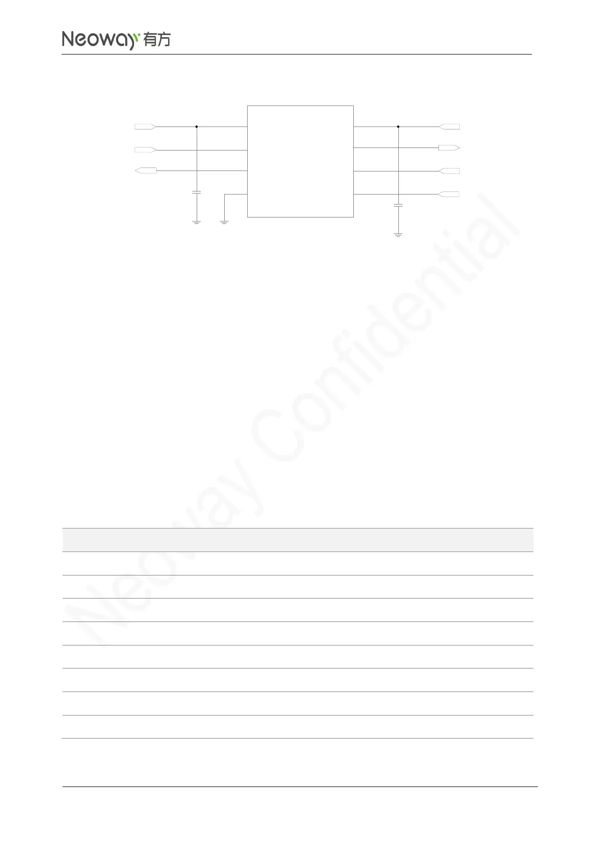
NLSX4373 is a dual-supply level shifter, the rate of which can be up to 20 Mb/s.
⚫
VL is the reference voltage of IO_VL1 and IO_VL2, ranging from 1.5V to 5.5V.
⚫
VCC is the reference voltage of IO_VCC1 and IO_VCC2, ranging from 1.5V to 5.5V.
⚫
EN is the enable pin, which works at a voltage of greater than VL-0.2V. In the above circuit, the
EN pin is connected to VDD_1P8 and the level shifter is always working.
PCB Design Guidelines
⚫
Do not cross other traces if possible. If crossing is inevitable, route the UART traces
perpendicular to other traces.
⚫
Keep traces far away from areas that might introduce ESD.
⚫
Surround the traces with the ground plane if possible.
3.3.5 SDC