EasyManua.ls Logo

Neoway N75 - Figure 3-38 SGMII Connection

Neoway N75
95 pages
Print Icon
To Next Page IconTo Next Page
To Previous Page IconTo Previous Page
Loading...
N75
Hardware User Guide
Copyright © Neoway Technology Co., Ltd
45
Figure 3-38 SGMII connection
SGMII_TX_P
SGMII_TX_N
SGMII_RX_P
SGMII_RX_N
N75 module
C1
0.1μF
C2
0.1μF
C3 0.1μF
C4 0.1μF
SGMII_RX_P
SGMII_RX_N
SGMII_TX_P
SGMII_TX_N
PHY chipset
Schematic Guidelines
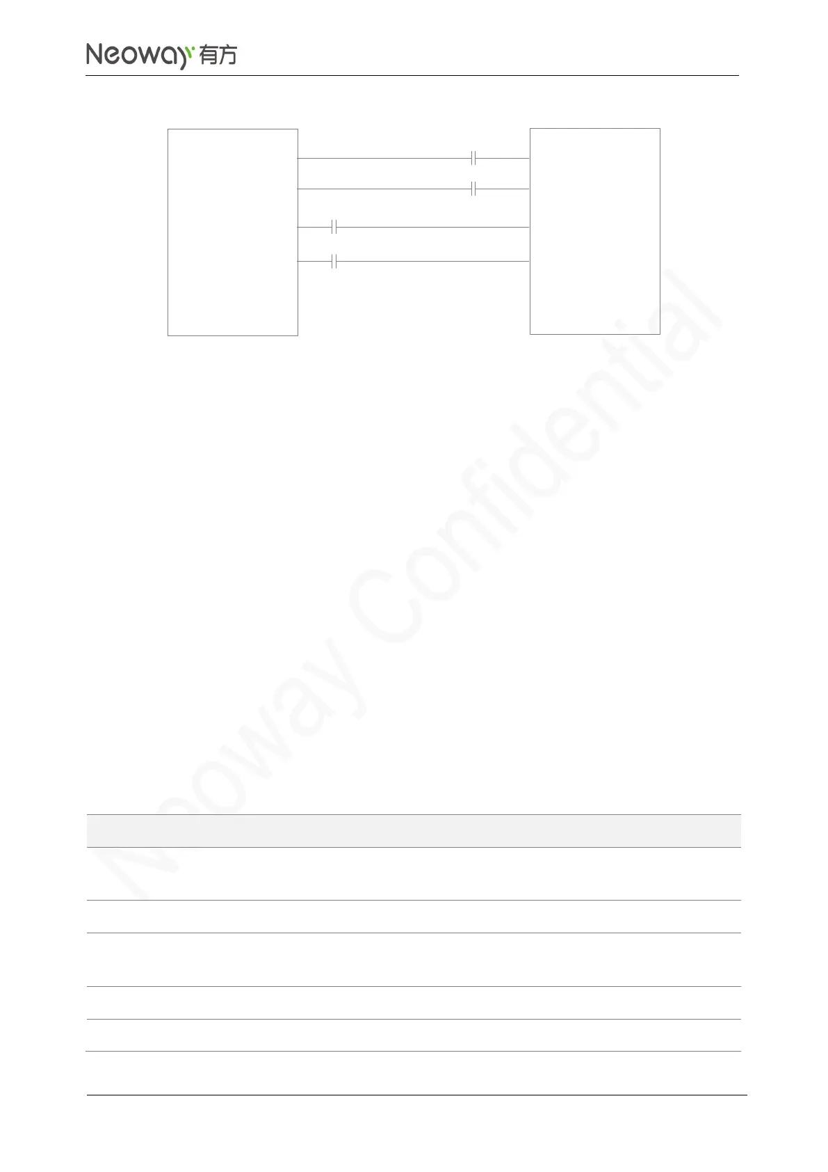
Note the match of SGMII signals.
Connect 0.1 μF DC blocking capacitors to SGMII pins in series.
PCB Design Guidelines
Place these DC blocking capacitors close to the RX pins on the PCB, e.g. C1 and C2 close to
the PHY chipset while C3 and C4 close to the module.
Keep the length difference of TX positive and negative signal lines. The difference should be
within 0.7mm.
Keep the length difference of RX positive and negative signal lines. The difference should be
within 0.7mm.
Control the impedance of the TX and RX traces separately, and the differential impedance
ranges from 80Ω to 120Ω.
Trace spacing between TX and RX should be 3x trace widths. Trace spacing between SGMII
and other traces should be 3x trace widths.
MDIO and PHY
Signal
Pin
I/O
Function
Remarks
USIM2_VCC
21
PO
Power supply for MDIO data
line to be pulled up to
Compatible with 1.8 V/3 V UIM
card
SGMII_MDIO_CLK
22
DO
MDIO clock
SGMII_MDIO_DATA
23
B
MDIO data IO
Add a 1.5kΩ resistor between
this pin and UIM2_VCC.
ETH_REST_N
24
DO
Ethernet PHY chipset reset
ETH_INT_N
25
DI
Ethernet PHY chipset interrupt

Table of Contents

Related product manuals