Schematic Guidelines
⚫
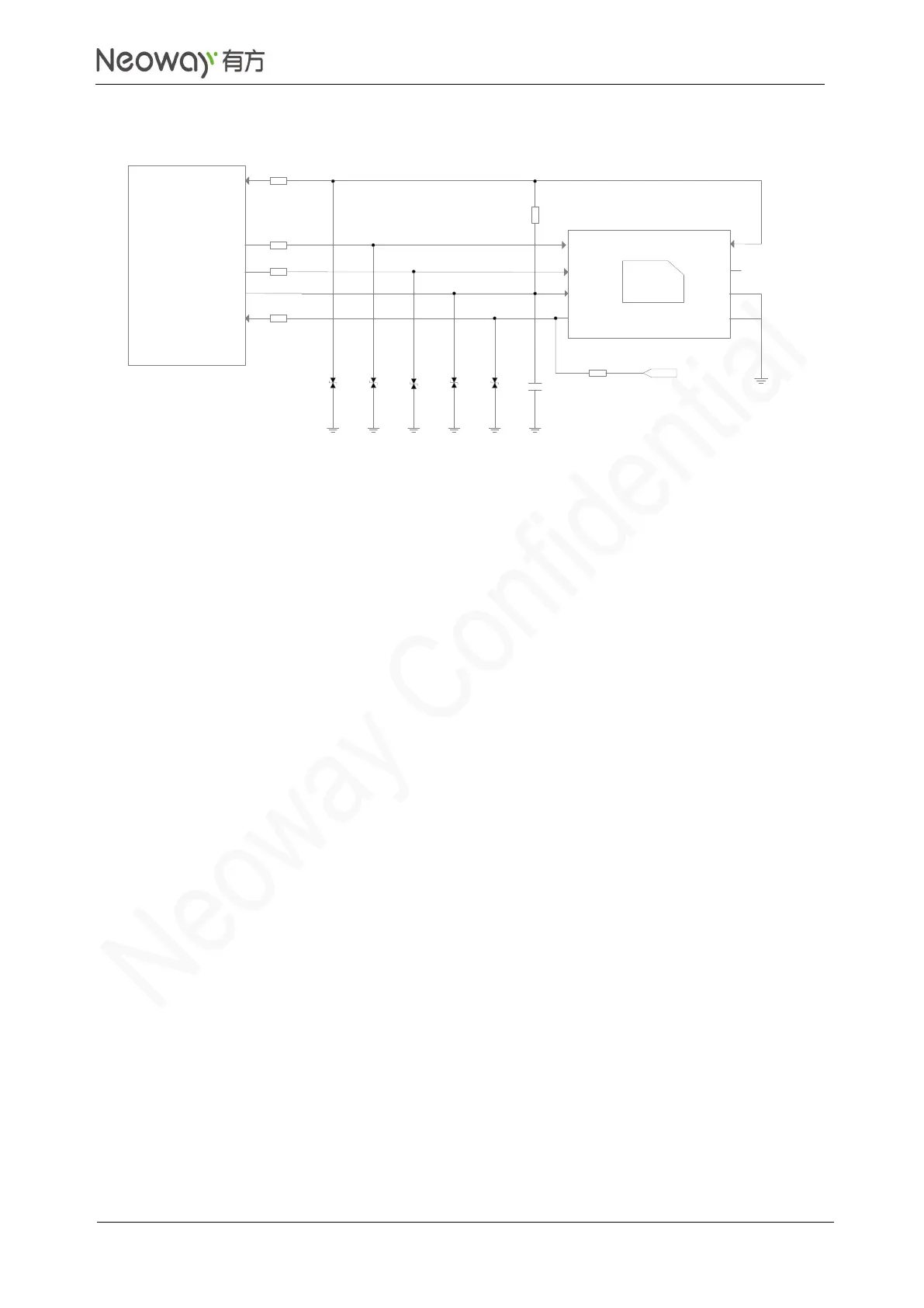
This reference design is applicable to USIM1 and USIM2 as well as USIM card and chipset.
⚫
Reserve a position for pull-up resistor externally in design since the USIM_DATA pin is not pulled
up internally.
⚫
USIM_VCC is the pin to supply power for SIM card and its maximum load is 30 mA. Do not use it
for any other purpose.
⚫
USIM_CLK is the clock signal pin, supporting a clock frequency of 3.25 GHz.
⚫
Add ESD protectors, such as ESD diodes or TVS diodes (with a junction capacitance less than
33pF) on the USIM signal lines in applications with a high requirement of ESD protection.
⚫
Connect a 20 Ω resistor respectively to USIM_DATA, USIM_RESET, USIM_CLK, and
USIM_DET in series to enhance the ESD performance.
⚫
N75 supports USIM card detection. USIM_DET is a 1.8V interrupt pin.
The UIM detection circuit works by checking the levels across the USIM_DET pin before and
after a UIM card is inserted. In the reference circuit, USIM-DET is floating before a USIM card is
inserted and is grounded after a USIM card is inserted. Low level means USIM card detected
while high level mean no USIM card detected.
PCB Design Guidelines
⚫
Place USIM far away from RF circuits. USIM signals are likely to be jammed by RF radiation,
resulting in failure to detect the SIM card.
⚫
Place USIM card close to the module and USIM traces should be as short as possible.
⚫
Place ESD protection resistors and components close to USIM card.
⚫
Surround USIM traces with ground to enhance EMC capability.