⚫
The maximum input voltage for the module is 4.3V and the typical value is 3.8 V.
⚫
The recommended protection voltage is 5V, to clamp the surge voltage before it enters back-end
circuits. Therefore, the back-end components and the module will not be damaged.
⚫
A large bypass tantalum capacitor (220 μF or 100 μF) or aluminum capacitor (470 μF or 1000
μF) is expected at C1 to reduce voltage drops during bursts together with C2, a 10 μF ceramic
capacitor. Its maximum safe operating voltage should be larger than 1.5 times the voltage across
the power supply.
⚫
Place low-ESR bypass capacitors at C3 (0.1 μF), C4 (100 pF), and C5 (33 pF) to filter out high-
frequency noise from the power supply.
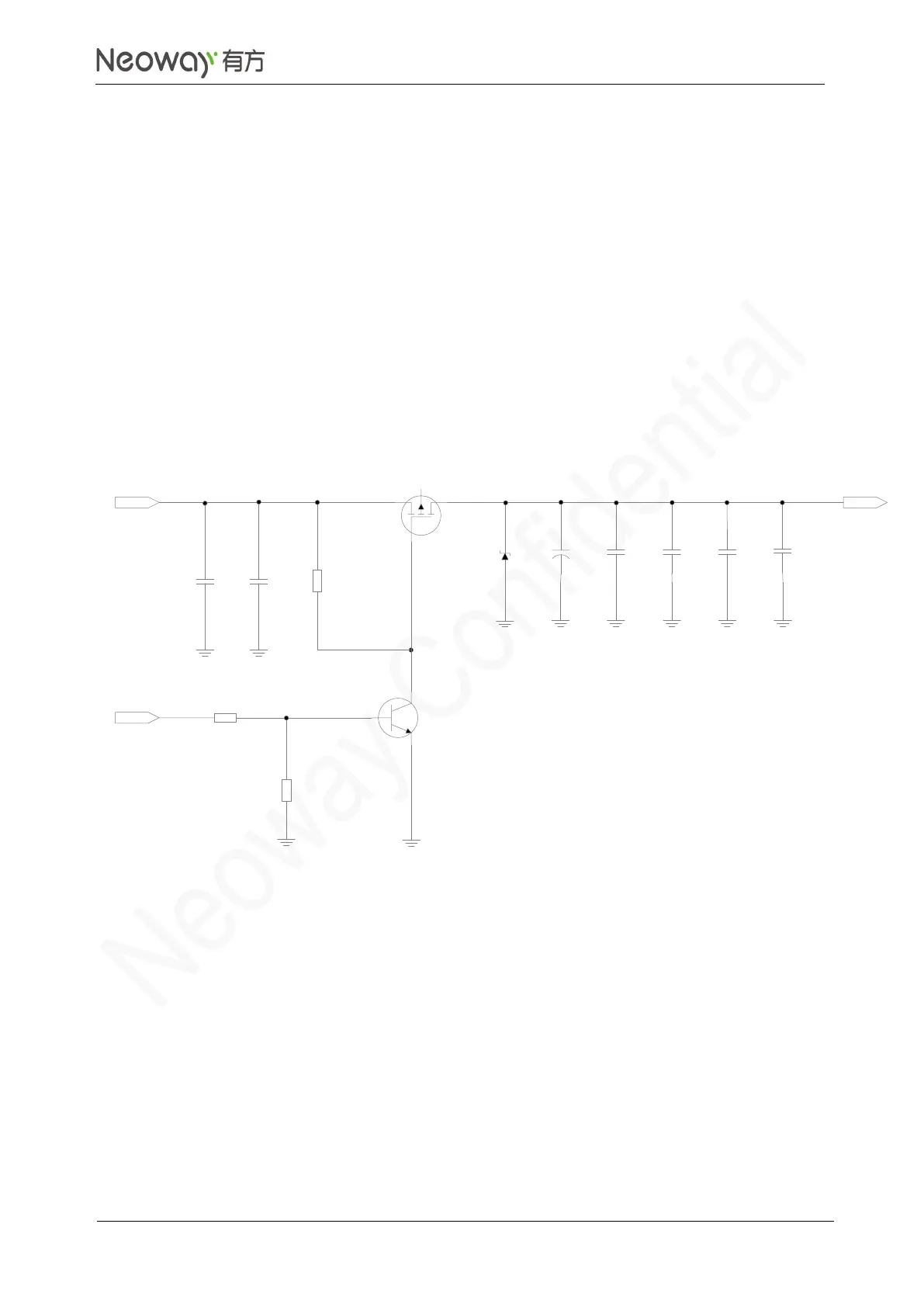
A controllable power supply is preferable if the module is used in harsh conditions. Figure 3-3 shows
the recommended schematic design.
Figure 3-3 Recommended design 2
⚫
Select an enhanced p-MOSFET at Q1, which has higher withstand voltage and 3A drain current
and low Rds.
⚫
Select a common NPN bipolar transistor at Q2. Please note the values of R1 and R2. Reserve
redundancy in these two values in case that the transistor requires higher voltage at base to
switch on in low temperature. If a digital NPN bipolar transistor is used, Omit R1 and R2.
⚫
TVS diodes work in the same way as those in Figure 3-2 and they should meet the same
requirements.
Figure 3-4 shows schematic design recommended for 4.3V-5.5V input.