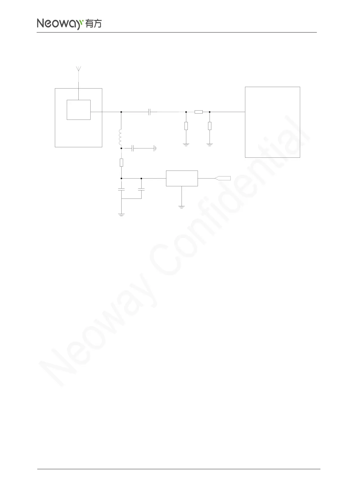
Schematic Guidelines
⚫
Use a low noise LDO dedicated for RF to supply power for the active antenna.
⚫
R1 is a current limit resistor. Its resistance is determined by the operating voltage and current of
the active antenna and the output voltage of LDO. Common active antenna requires 3.3V to 5V
power supply.
⚫
L1 and C2 form an LC filter to clamp current and filter out high-frequency jamming signal. An
inductor of 47 nH to 100 nH is recommended at L1.
⚫
C1 is a DC blocking capacitor and its capacitance is 33 pF or 100 pF.
Z1, Z2, and Z3 form a matching network, see section 3.5.1 ANT_MAIN/ANT_DIV antenna
interface.
PCB Design Guidelines
⚫
For PCB design guidelines between GNSS interface and antenna, refer to design guidelines in
section 3.5.1 ANT_MAIN/ANT_DIV antenna interface.
⚫
50Ω impedance is required for the feeder and PCB traces and the traces should be as short as
possible.
⚫
Do NOT connect one end of L1 to the GNSS signal impedance lines directly.
⚫
Keep GNSS antenna circuit far away from the main/diversity antenna circuits on PCB.
Otherwise, these two parts will jam each other, lowing the RF performance.
Figure 3-53 shows reference layout of GNSS antenna traces. This design is also applicable to