2.85V, connect to VCC of the SD card. If the IO is 1.8V, connect to the VDD_1P8 pin of the
module.
⚫
The recommended supply voltage of VCC ranges 2.85V to 3.0V and current is larger than 500
mA. An LDO or DC-DC is recommended.
⚫
Connect a resistor of 15Ω to 24Ω to SDC_CLK in series.
⚫
The SD card detection function is implemented by the interrupt, which is triggered by level
change at the SDC_DET pin after an SD card is installed in the card connector. As shown in
Figure 3-21, SDC_DET is left floating before an SD card is inserted and grounded after an SD
card is inserted, and the level at SDC_DET changes from high to low.
⚫
Add an ESD protector of lower than 10 pF to each pin. ESD protection diode array is an option.
In Figure 3-21, ESD1 and ESD2 consist of four same ESD protectors.
PCB Design Guidelines
⚫
Place ESD protectors close to SD connector. The pin numbers of ESD arrays can be adjusted in
actual applications.
⚫
The trace of power supply should be wider than 0.5 mm.
⚫
Place the resistor on the CLK line close to the module.
⚫
Control the length difference of DATA, CMD, and CLK signal traces to 1 mm.
⚫
Keep the total length of DATA, CMD, and CLK signal traces to 40 mm.
⚫
Spacing between CMD, CLK, and DATA traces should be larger than 2 times trace width.
⚫
Spacing between CMD, CLK, and DATA traces and other signal traces should be larger than 2
times trace width.
⚫
Control the impedance for CMD, CLK, and DATA traces to 50Ω individually.
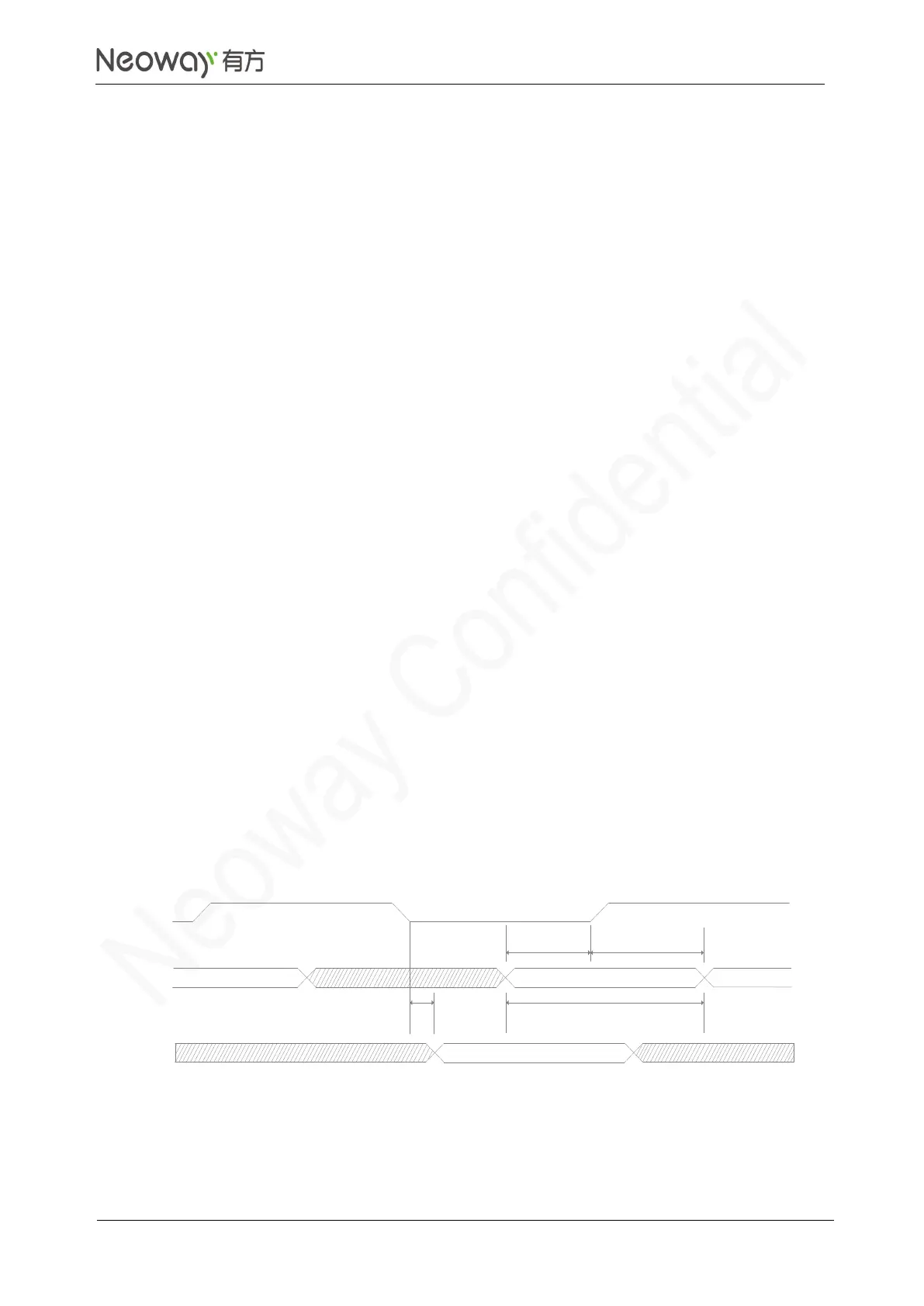
For the timing of the SDC interface in SDR and DDR mode, see Figure 3-22 and Figure 3-23. For
parameter values for the SD interface, see Table 3-4.
Figure 3-22 SDC SDR timing