Schematic Guidelines
⚫
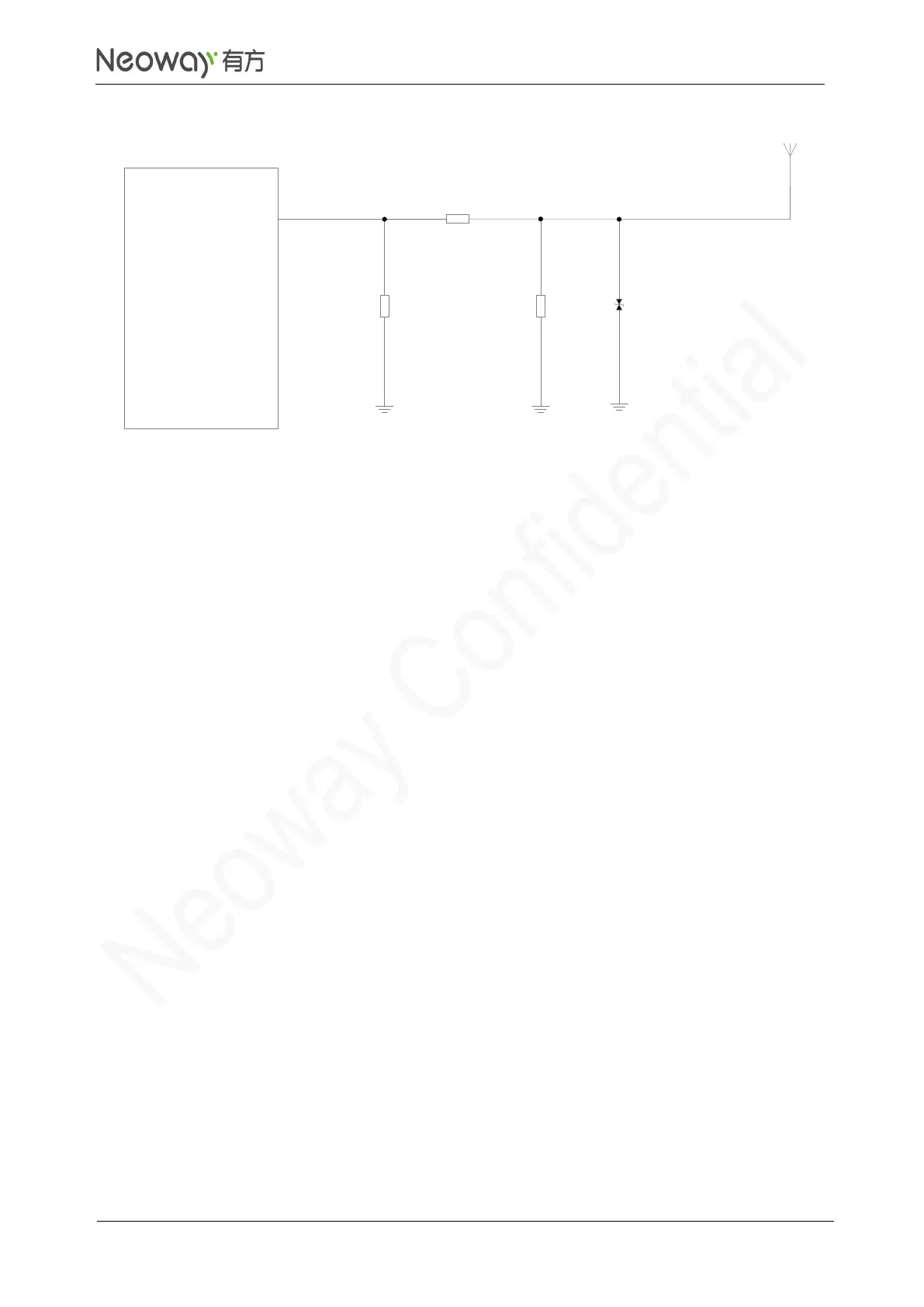
Element components in the above figures should be capacitors, inductors, and 0Ω resistors.
Place these RLC components as close to the antenna interface as possible.
⚫
Recommended RLC values:
In Figure 3-46, Z1=47nH, Z2=100pF;
In Figure3-47, Z1=0Ω, Z2=47nH, Z3=100pF;
In Figure3-48, Z1=47nH, Z2=100pF, Z3=NC.
⚫
Add an ESD protector if the antenna might generate static electricity. The protector can be an
ESD protector with a junction capacitance of lower than 0.5 pF. Ensure that the reverse
breakdown voltage of the ESC protector is greater than 10V (above 15 V is recommended).
PCB Design Guidelines
⚫
Lay copper foil around RF connector. Dig as many ground holes as possible on the copper to
ensure lowest grounding impedance.
⚫
The trace between N75 and the antenna connector, should be as short as possible. Control the
trace impedance to 50Ω.
⚫
Keep clean space (2 times trace width) at both sides of traces.
⚫
If customers adopt SMA connector, big RF solder pad might result in great parasitic capacitance,
which will affect the antenna performance. Remove the copper on the first and second layers
under the RF solder pad.
⚫
Note the distance between ANT_MAIN and ANT_DIV in case of EMI jamming to each other.
⚫
On the PCB, keep the RF signals and components far away from high-speed circuits, power
supplies, transformers, great inductors, the clock circuit, etc.