Oki Data CONFIDENTIAL
44871001TH Rev.6
10-22
10. APPENDIX
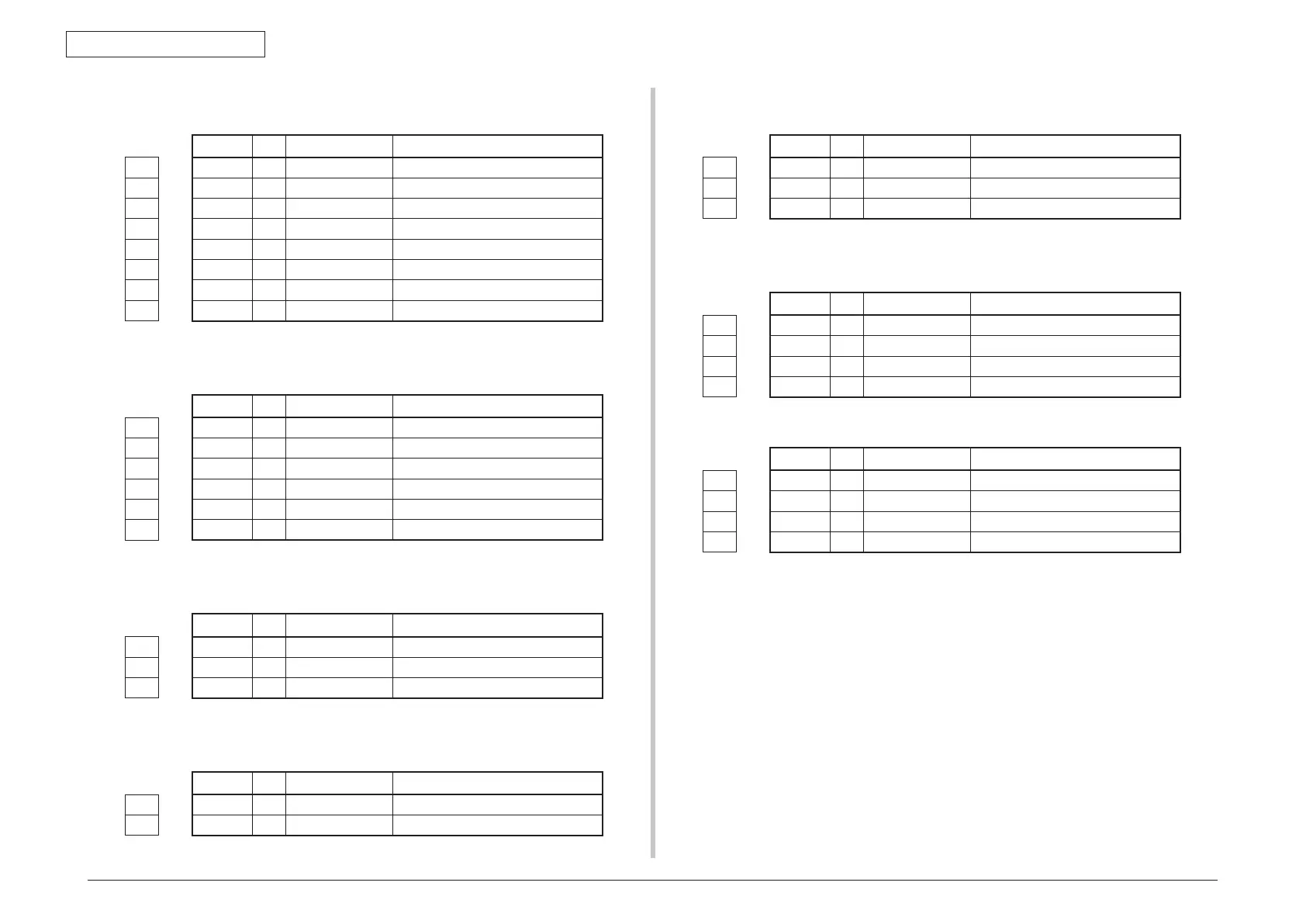
• MAIN1ConnectorPinAllocation
(Connection to the Main control board)
PIN No. I/O Signal Function
1 1 C 0VP Analog Ground
2 2 O 24V Motor/ Clutch Drive Power
3 3 C 0VL Logic Ground
4 4 I +5V Logic Circuit Power supply
5 5 O OPTSCK-N OPT data output
6 6 I OPTSD-P OPT data input
7 7 O OPTSDR-N OPT status change
8 8 I OPTPSIN-N OPT transfer permission
• SNS03ConnectorPinAllocation
(Connection to the Hopping / Paper end sensor)
PIN No. I/O Signal Function
1 1 O +5V Logic Circuit Power supply
2 2 I SNS3-N Hopping sensor
3 3 C 0VL Logic Ground
4 4 O +5V Logic Circuit Power supply
5 5 I SNS0-N Paper end sensor
6 6 C 0VL Logic Ground
• SNS12ConnectorPinAllocation
(Connection to the Entrance sensor)
PIN No. I/O Signal Function
1 1 O +5V Logic Circuit Power supply
2 2 I SNS1-N Entrance sensor
3 3 C 0VL Logic Ground
• CL1ConnectorPinAllocation
(Connection to the Regist clutch)
PIN No. I/O Signal Function
1 1 O 24V Motor/ Clutch Drive Power
2 2 C CLUTCH1 Analog Ground
• CL2ConnectorPinAllocation
(Connection to the Feed clutch)
PIN No. I/O Signal Function
1 1 O POW Motor/ Clutch Drive Power
2 2 C CLUTCH2 Analog Ground
3 3 - NC Not used
• MOTORConnectorPinAllocation
(Connection to the Pulse motor)
PIN No. I/O Signal Function
1 1 O HOP4 Motor Drive Power
2 2 O HOP3 Motor Drive Power
3 3 O HOP2 Motor Drive Power
4 4 O HOP1 Motor Drive Power
• FLASHConnectorPinAllocation
PIN No. I/O Signal Function
1 1 I/O MODE Serial Data
2 2 I RESET Reset
3 3 C 0VL Logic Ground
4 4 O VCC_CPU Logic Circuit Power supply(+3.3)