Creating Programs
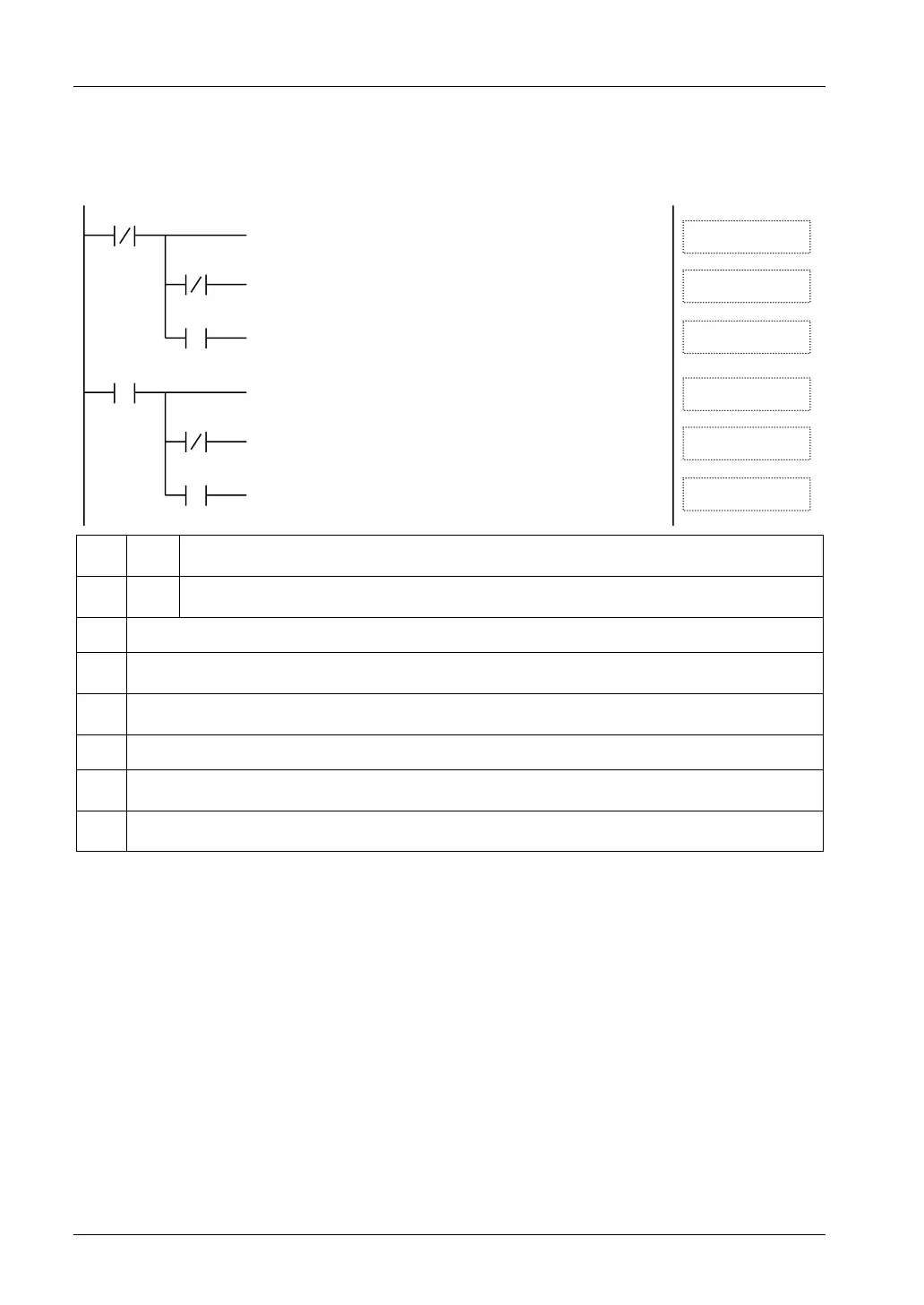
Sample program (FP0R-A42: For ranges of -10 V to +10 V and -5 V to +5 V)
The following program shows the case that conversion data of the first expansion analog I/O
unit (FP0R-A42) (CH0 to CH3) is read and stored in DT0 to DT3.
[ F0 MV , WX2 , DT0 ]
[ F65 WAN , WX3 , H3FFF , DT1 ]
X3E
X3D
②
ⓐ
①
[ F66 WOR , WX3 , HC000 , DT1 ]
X3D
②
ⓑ
ⓒ
[ F65 WAN , WX3 , H3FFF , DT3 ]
[ F0 MV , WX2 , DT2 ]
X3E
X3D
②
ⓓ
①
[ F66 WOR , WX3 , HC000 , DT3 ]
X3D
②
ⓔ
ⓕ
①
X3E
The channels of conversion data read by turning on/off the conversion data switching flag X3E
are distinguished.
②
X3D
The signs of read conversion data of CH1/CH3 are distinguished. When plus, OFF. When minus,
ON.
ⓐ
The conversion data of CH0 is transferred to DT0.
ⓑ
When the data of CH1 is positive, the most significant two bits are masked by "00" with F65 WAN (AND)
instruction, and the data is stored in DT1.
ⓒ
When the data of CH1 is negative, the most significant two bits are masked by "11" with F66 WOR (OR)
instruction, and the data is stored in DT1.
ⓓ
The conversion data of CH2 is transferred to DT2.
ⓔ
When the data of CH3 is positive, the most significant two bits are masked by "00" with F65 WAN (AND)
instruction, and the data is stored in DT3.
ⓕ
When the data of CH3 is negative, the most significant two bits are masked by "11" with F66 WOR (OR)
instruction, and the data is stored in DT3.
 Loading...