User Manual
E727T0005, valid for E-727
BRO, 2019-06-28
Physik Instrumente (PI) GmbH & Co. KG, Auf der Roemerstrasse 1, 76228 Karlsruhe, Germany Page 161 / 240
Phone +49 721 4846-0, Fax +49 721 4846-1019, Email info@pi.ws, www.pi.ws
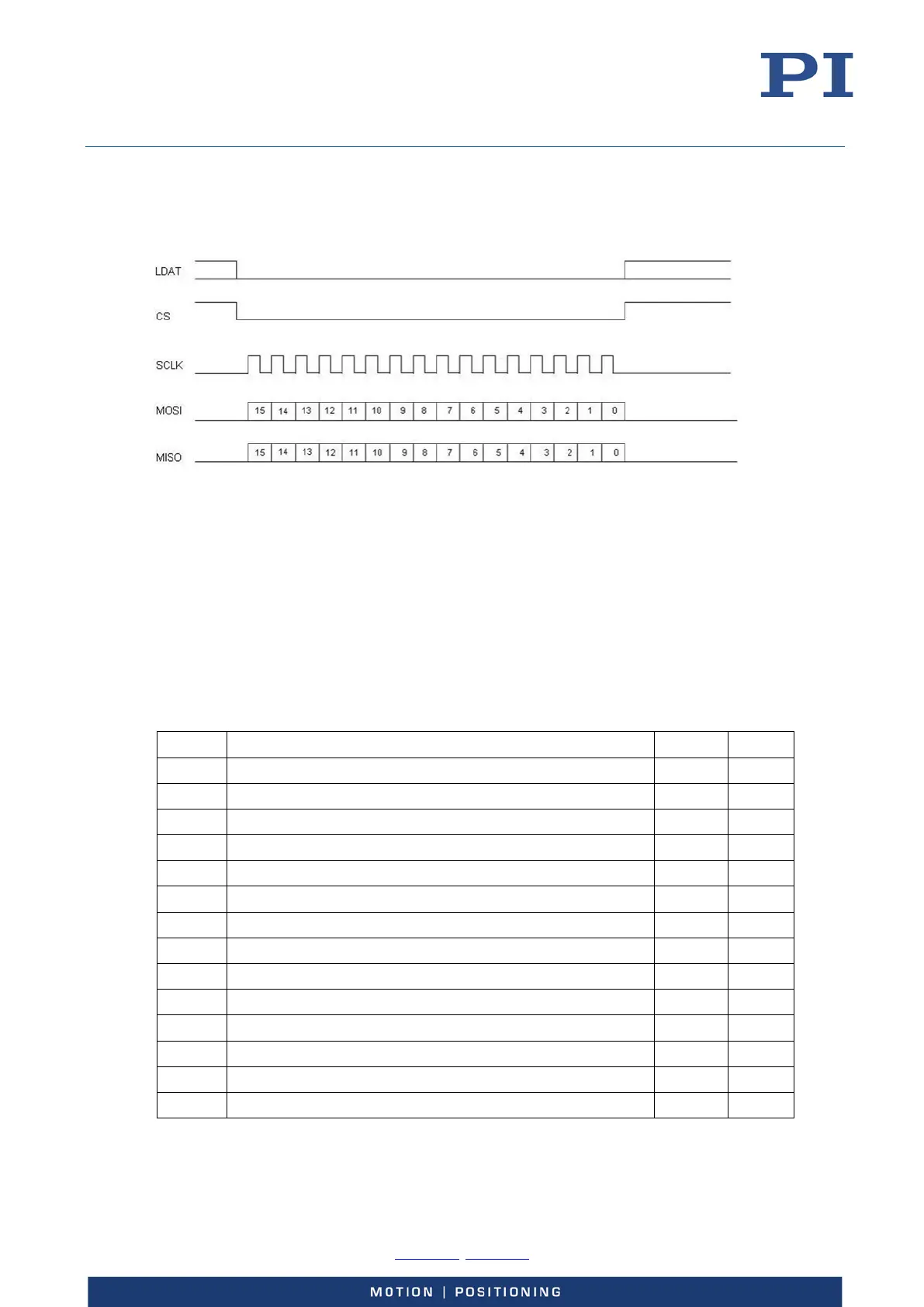
The following diagram shows the transfer of one single 16-bit data word. All bytes of a packet are
transferred serially with the highest bit first. The data bits of the MISO line change with the rising
edge of SCLK. The data bits of the MOSI line are latched with the negative edge of SCLK. The SCLK
line is active only while data bits are transferred.
Physical Layer
Transmission Lines
Each signal is transmitted by a differential data line pair. For the pin assignment, see p. 233.
The electrical level is LVDS. On receiver side each line must be terminated with 100 ohm.
Timing Diagrams
Note that the time values depend on controller type. The time values listed below were measured
at the connector of E-727.
Symbol Description Min Max
TSLO SCLK low time 7 ns
TSPD SCLK period time 15 ns
Input setup time: MOSI-bit valid before falling edge of SCLK
TIHD Input hold time: MOSI-bit valid after falling edge of SCLK 0 ns
TSUS Output setup time: MISO-bit valid after rising edge of SLCK 15 ns
TSDD SCLK to DCLK delay time 10 ns
TSUD Output setup time: MISO-bit valid after rising edge of DLCK 6 ns
TFLS Falling edge of LDAT before first rising edge of SCLK 0 ns
TSRL Last falling edge of SCLK before rising edge of LDAT 0 ns
LDAT high: Time between two commands
TFCS Falling edge of CS before rising edge of SCLK N/A N/A
TSRC Falling edge of SCLK before rising edge of CS N/A N/A
TCSH CS high: Time between two 16-bit data words N/A N/A