RL78/G13 CHAPTER 9 CLOCK OUTPUT/BUZZER OUTPUT CONTROLLER
R01UH0146EJ0100 Rev.1.00 463
Sep 22, 2011
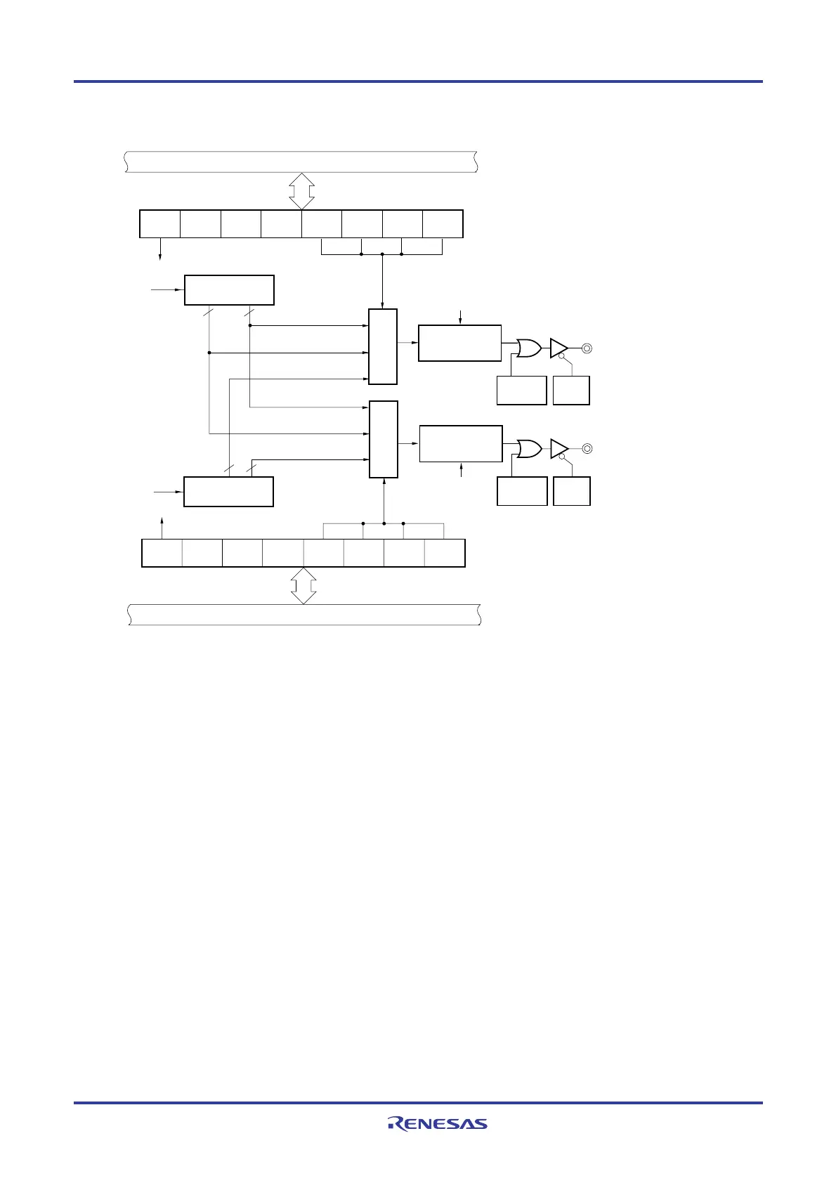
Figure 9-1. Block Diagram of Clock Output/Buzzer Output Controller
f
MAIN
f
SUB
PCLOE0 0 0 0
PCLOE0
5
3
PCLBUZ0
Note
/INTP6/P140
PCLBUZ1
Note
/INTP7/P141
CSEL0 CCS02 CCS01 CCS00
PM141
PM140
PCLOE1 0 0 0 CSEL1 CCS12 CCS11 CCS10
8
PCLOE1
8
f
MAIN
/2
11
to f
MAIN
/2
13
Clock/buzzer
controller
Internal bus
Clock output select register 1 (CKS1)
Prescaler
Prescaler
Selector
Selector
Clock/buzzer
controller
Output latch
(P141)
Internal bus
Clock output select register 0 (CKS0)
Output latch
(P140)
f
MAIN
/2
11
to f
MAIN
/2
13
f
MAIN
to f
MAIN
/2
4
f
MAIN
to f
MAIN
/2
4
f
SUB
to f
SUB
/2
7
f
SUB
to f
SUB
/2
7
Note For output frequencies available from PCLBUZ0 and PCLBUZ1, refer 29.5 AC Characteristics.
Remark The clock output/buzzer output pins in above diagram shows the information of 64- to 128-pins products
with PIOR3 = 0 and PIOR4 = 0.
In other cases, the name of pins, output latches (Pxx) and PMxx should be read differently (xx = 15, 31, 55,
140 or 141).
<R>
<R>
 Loading...


