RL78/G13 CHAPTER 25 FLASH MEMORY
R01UH0146EJ0100 Rev.1.00 938
Sep 22, 2011
An overview of the data flash memory is provided below.
• The data flash memory can be written to by using the flash memory programmer or an external device
• Programming is performed in 8-bit units
• Blocks can be deleted in 1 KB units
• The only access by CPU instructions is byte reading (reading: four clock cycles)
• Because the data flash memory is an area exclusively used for data, it cannot be used to execute instructions (code
fetching)
• Instructions can be executed from the code flash memory while rewriting the data flash memory (That is, back ground
operation (BGO) is supported)
• Accessing the data flash memory is not possible while rewriting the code flash memory (during self programming)
• Because the data flash memory is stopped after a reset ends, the data flash control register (DFLCTL) must be set
up in order to use the data flash memory
• Manipulating the DFLCTL register is not possible while rewriting the data flash memory
• When data flash is accessed, the CPU waits for three clock cycles
25.4.2 Register controlling data flash memory
(1) Data flash control register (DFLCTL)
This register is used to enable or disable accessing to the data flash.
The DFLCTL register is set by a 1-bit or 8-bit memory manipulation instruction.
Reset input sets this register to 00H.
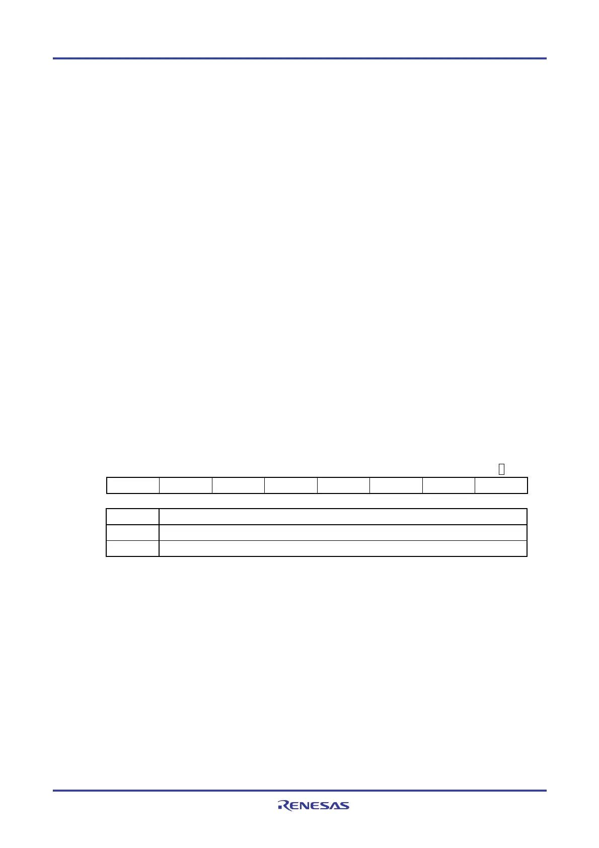
Figure 25-6. Format of Data Flash Control Register (DFLCTL)
Address: F0090H After reset: 00H R/W
Symbol 7 6 5 4 3 2 1
0
DFLCTL 0 0 0 0 0 0 0 DFLEN
DFLEN Data flash access control
0 Disables data flash access
1 Enables data flash access
Caution Manipulating the DFLCTL register is not possible while rewriting the data flash memory.
<R>
<R>

 Loading...


