RL78/G13 CHAPTER 3 CPU ARCHITECTURE
R01UH0146EJ0100 Rev.1.00 133
Sep 22, 2011
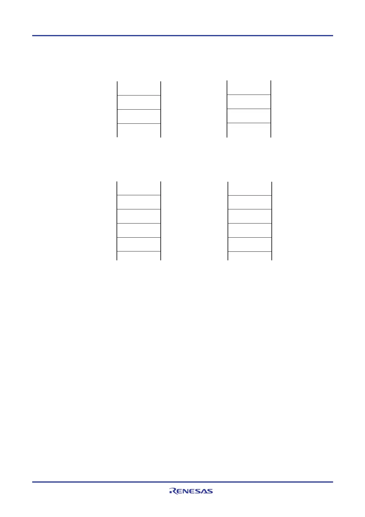
Figure 3-25. Data to Be Saved to Stack Memory
PC7 to PC0
PC15 to PC8
PC19 to PC16
PSW
Interrupt, BRK instruction
SP←SP−4
↑
SP−4
↑
SP−3
↑
SP−2
↑
SP−1
↑
SP →
CALL, CALLT instructions
Register pair lower
Register pair higher
PUSH rp instruction
SP←SP−2
↑
SP−2
↑
SP−1
↑
SP →
(4-byte stack)
(4-byte stack)
PC7 to PC0
PC15 to PC8
PC19 to PC16
00H
SP←SP−4
↑
SP−4
↑
SP−3
↑
SP−2
↑
SP−1
↑
SP →
00H
PSW
PUSH PSW instruction
SP←SP−2
↑
SP−2
↑
SP−1
↑
SP →
3.2.2 General-purpose registers
General-purpose registers are mapped at particular addresses (FFEE0H to FFEFFH) of the data memory. The general-
purpose registers consists of 4 banks, each bank consisting of eight 8-bit registers (X, A, C, B, E, D, L, and H).
Each register can be used as an 8-bit register, and two 8-bit registers can also be used in a pair as a 16-bit register (AX,
BC, DE, and HL).
These registers can be described in terms of function names (X, A, C, B, E, D, L, H, AX, BC, DE, and HL) and absolute
names (R0 to R7 and RP0 to RP3).
Register banks to be used for instruction execution are set by the CPU control instruction (SEL RBn). Because of the 4-
register bank configuration, an efficient program can be created by switching between a register for normal processing and
a register for interrupts for each bank.
Cautions 1. It is prohibited to use the general-purpose register (FFEE0H to FFEFFH) space for fetching
instructions or as a stack area.
2. The internal RAM in the following products cannot be used as stack memory when using the self-
programming function and data flash function.
R5F100xD, R5F101xD (x = 6 to 8, A to C, E to G, J, L): FF300H to FF309H
R5F100xE, R5F101xE (x = 6 to 8, A to C, E to G, J, L): FEF00H to FF309H
R5F100xJ, R5F101xJ (x = F, G, J, L, M, P): FAF00H to FB309H
R5F100xL, R5F101xL (x = F, G, J, L, M, P, S): F7F00H to F8309H
<R>