RL78/G13 CHAPTER 4 PORT FUNCTIONS
R01UH0146EJ0100 Rev.1.00 175
Sep 22, 2011
4.2.2 Port 1
Port 1 is an I/O port with an output latch. Port 1 can be set to the input mode or output mode in 1-bit units using port
mode register 1 (PM1). When the P10 to P17 pins are used as an input port, use of an on-chip pull-up resistor can be
specified in 1-bit units by pull-up resistor option register 1 (PU1).
Input to the P10, P11, and P13 to P17 pins can be specified through a normal input buffer or a TTL input buffer in 1-bit
units using port input mode register 1 (PIM1).
Output from the P10 to P15 and P17 pins can be specified as N-ch open-drain output (V
DD tolerance) in 1-bit units
using port output mode register 1 (POM1).
This port can also be used for serial interface data I/O, clock I/O, programming UART I/O, timer I/O, and external
interrupt request input.
Reset signal generation sets port 1 to input mode.
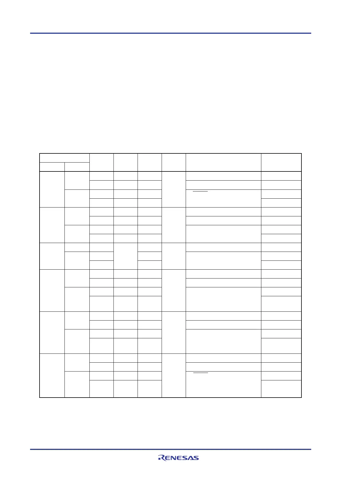
Table 4-4. Settings of Registers When Using Port 1 (1/2)
Pin Name
Name I/O
PM1× PIM1× POM1× PMC××
Alternate Function Setting
Note 10
Remark
1
0
Note 1
× − ×
CMOS input
Input
1
1
Note 1
×
×
TTL input
0
×
0
Note 1
CMOS output
P10
Output
0
×
1
Note 1
SCK00/SCL00 output = 1
Note 2
(TO07 output = 0
Note 7
)
N-ch O.D. output
1
0
Note 1
× − ×
CMOS input
Input
1
1
Note 1
×
×
TTL input
0
×
0
Note 1
CMOS output
P11
Output
0
×
1
Note 1
SDA00 output = 1
Note 2
(TO06 output = 0
Note 7
)
N-ch O.D. output
Input 1
− × − ×
CMOS input
0 0 CMOS output
P12
Output
0 1
SO00/TxD1 output = 1
Note 2
(TO05 output = 0
Note 7
)
N-ch O.D. output
1 0
× − ×
CMOS input Input
1 1
×
×
TTL input
0
×
0 CMOS output
P13
Output
0
×
1
TxD2/SO20 output = 1
Note 2
(TO04 output = 0
Note 7
,
SDAA0 output = 0
Note 8
)
N-ch O.D. output
1 0
× − ×
CMOS input Input
1 1
×
×
TTL input
0
×
0 CMOS output
P14
Output
0
×
1
SDA20 output = 1
Note 2
(TO03 output = 0
Note 7
,
SCLA0 output = 0
Note 8
)
N-ch O.D. output
1 0
× − ×
CMOS input Input
1 1
×
×
TTL input
0
×
0 CMOS output
P15
Output
0
×
1
SCK20/SCL20 output = 1
Note 2
PCLBUZ1 output = 0
Note 7
(TO02 output = 0
Note 8
)
N-ch O.D. output
(Notes and Remark are listed on the next page.)
<R>

 Loading...


