RL78/G13 CHAPTER 24 OPTION BYTE
R01UH0146EJ0100 Rev.1.00 927
Sep 22, 2011
24.3 Format of On-chip Debug Option Byte
The format of on-chip debug option byte is shown below.
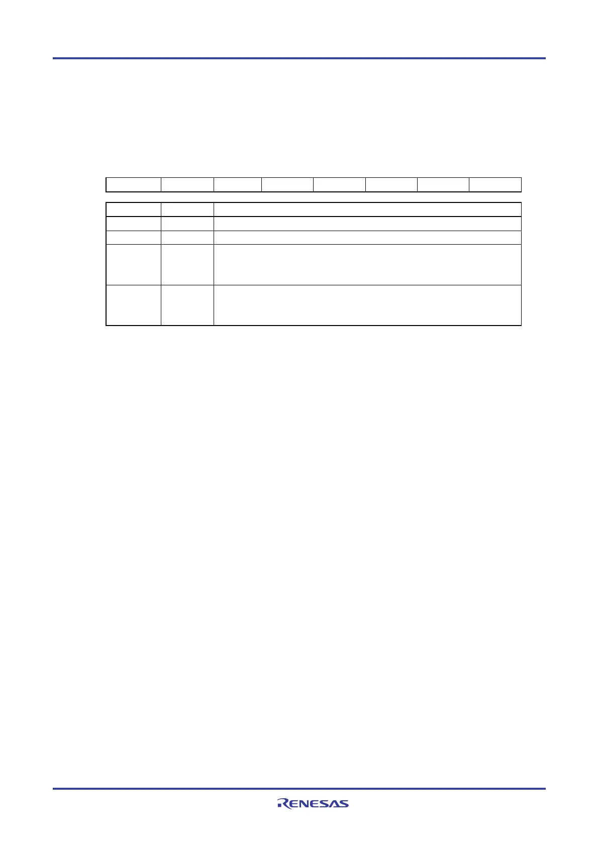
Figure 24-4. Format of On-chip Debug Option Byte (000C3H/010C3H)
Address: 000C3H/010C3H
Note
7 6 5 4 3 2 1 0
OCDENSET 0 0 0 0 1 0 OCDERSD
OCDENSET OCDERSD Control of on-chip debug operation
0 0 Disables on-chip debug operation.
0 1 Setting prohibited
1 0 Enables on-chip debugging.
Erases data of flash memory in case of failures in authenticating on-chip debug
security ID.
1 1 Enables on-chip debugging.
Does not erases data of flash memory in case of failures in authenticating on-chip
debug security ID.
Note Set the same value as 000C3H to 010C3H when the boot swap operation is used because 000C3H is replaced
by 010C3H.
Caution Bits 7 and 0 (OCDENSET and OCDERSD) can only be specified a value.
Be sure to set 000010B to bits 6 to 1.
Remark The value on bits 3 to 1 will be written over when the on-chip debug function is in use and thus it will become
unstable after the setting.
However, be sure to set the default values (0, 1, and 0) to bits 3 to 1 at setting.

 Loading...


