RL78/G13 CHAPTER 1 OUTLINE
R01UH0146EJ0100 Rev.1.00 39
Sep 22, 2011
(2/2)
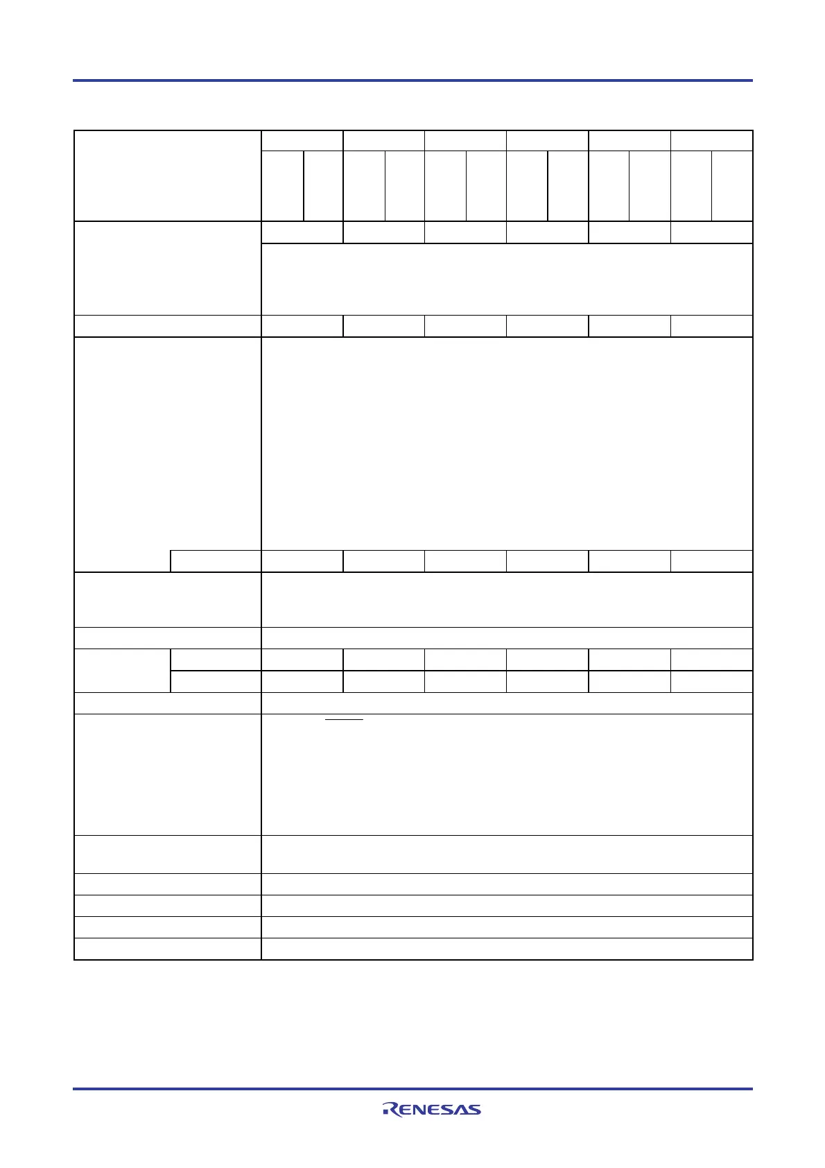
20-pin 24-pin 25-pin 30-pin 32-pin 36-pin Item
R5F1006x
R5F1016x
R5F1007x
R5F1017x
R5F1008x
R5F1018x
R5F100Ax
R5F101Ax
R5F100Bx
R5F101Bx
R5F100Cx
R5F101Cx
−
1 1 2 2 2
Clock output/buzzer output
• 2.44 kHz, 4.88 kHz, 9.76 kHz, 1.25 MHz, 2.5 MHz, 5 MHz, 10 MHz
(Main system clock: f
MAIN = 20 MHz operation)
• 256 Hz, 512 Hz, 1.024 kHz, 2.048 kHz, 4.096 kHz, 8.192 kHz, 16.384 kHz, 32.768 kHz
(Subsystem clock: f
SUB = 32.768 kHz operation)
8/10-bit resolution A/D converter 6 channels 6 channels 6 channels 8 channels 8 channels 8 channels
Serial interface [20-pin, 24-pin, 25-pin products]
• CSI: 1 channel/UART: 1 channel/simplified I
2
C: 1 channel
• CSI: 1 channel/UART: 1 channel/simplified I
2
C: 1 channel
[30-pin, 32-pin products]
• CSI: 1 channel/UART: 1 channel/simplified I
2
C: 1 channel
• CSI: 1 channel/UART: 1 channel/simplified I
2
C: 1 channel
• CSI: 1 channel/UART (UART supporting LIN-bus): 1 channel/simplified I
2
C: 1 channel
[36-pin products]
• CSI: 1 channel/UART: 1 channel/simplified I
2
C: 1 channel
• CSI: 1 channel/UART: 1 channel/simplified I
2
C: 1 channel
• CSI: 2 channel/UART (UART supporting LIN-bus): 1 channel/simplified I
2
C: 2 channel
I
2
C bus
−
1 channel 1 channel 1 channel 1 channel 1 channel
Multiplier and divider/multiply-
accumulator
• 16 bits × 16 bits = 32 bits (Unsigned or signed)
• 32 bits ÷ 32 bits = 32 bits (Unsigned)
• 16 bits × 16 bits + 32 bits = 32 bits (Unsigned or signed)
DMA controller 2 channels
Internal 23 24 24 27 27 27
Vectored interrupt
sources
External 3 5 5 6 6 6
Key interrupt
−
Reset
• Reset by RESET pin
• Internal reset by watchdog timer
• Internal reset by power-on-reset
• Internal reset by voltage detector
• Internal reset by illegal instruction execution
Note
• Internal reset by RAM parity error
• Internal reset by illegal-memory access
Power-on-reset circuit
• Power-on-reset: 1.51 ±0.03 V
• Power-down-reset: 1.50 ±0.03 V
Voltage detector 1.63 V to 4.06 V (14 stages)
On-chip debug function Provided
Power supply voltage VDD = 1.6 to 5.5 V
Operating ambient temperature TA = −40 to +85 °C
Note The illegal instruction is generated when instruction code FFH is executed.
Reset by the illegal instruction execution not issued by emulation with the in-circuit emulator or on-chip debug
emulator.

 Loading...


