RL78/G13 CHAPTER 13 SERIAL INTERFACE IICA
R01UH0146EJ0100 Rev.1.00 727
Sep 22, 2011
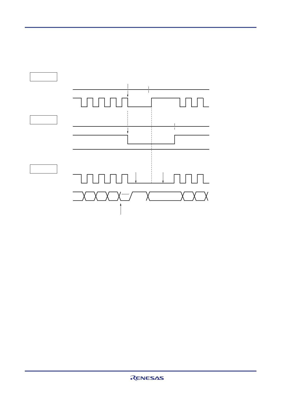
Figure 13-20. Wait (2/2)
(2) When master and slave devices both have a nine-clock wait
(master transmits, slave receives, and ACKE0 = 1)
Master
IICA0
SCLA0
Slave
IICA0
SCLA0
ACKE0
Transfer lines
SCLA0
SDAA0
H
6789 1 23
Master and slave both wait
after output of ninth clock
Wait from
master and
slave
Wait from slave
IICA0 data write (cancel wait)
FFH is written to IICA0 or WREL0 is set to 1
6789 123
D2 D1 D0 ACK D7 D6 D5
Generate according to previously set ACKE0 value
Remark ACKE0: Bit 2 of IICA control register 00 (IICCTL00)
WREL0: Bit 5 of IICA control register 00 (IICCTL00)
A wait may be automatically generated depending on the setting of bit 3 (WTIM0) of IICA control register 00 (IICCTL00).
Normally, the receiving side cancels the wait state when bit 5 (WREL0) of the IICCTL00 register is set to 1 or when
FFH is written to the IICA shift register 0 (IICA0), and the transmitting side cancels the wait state when data is written to
the IICA0 register.
The master device can also cancel the wait state via either of the following methods.
• By setting bit 1 (STT0) of the IICCTL00 register to 1
• By setting bit 0 (SPT0) of the IICCTL00 register to 1

 Loading...


