Configuration in STEP 7
5.9 Configuring time-of-day synchronization
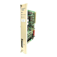
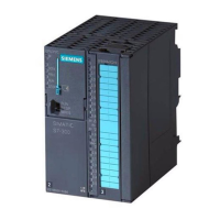
TIM DNP3
136 System Manual, 12/2015, C79000-G8976-C253-04
The TIM in the S7-300 makes the time of day available to its local CPU in the I/O addresses.
The CPU user program can then read and evaluate the time there.
The I/O addresses of the CPU that makes the date and time information available to the TIM
are set in the properties dialog of the TIM, "Addresses" tab; refer to the section "Addresses"
tab (Page 116).
The time information of a time-synchronized TIM module with TD7onTIM is stored in 8 bytes
of the peripheral inputs. The time information has an offset of 8 bytes from the start value of
the inputs. The following table shows the assignment of the 8 bytes of time information.
Table 5- 1 Format of the time information in the inputs of the I/O addresses of the TIM
Range of val-
ues (decimal)
Range of val-
ues (decimal)
3 +10
tens 0...9 ones 0...9
5 +12
tens 0...9 ones 0...9
Meaning of the entries in the table:
● Offset: Offset to the base value of the peripheral inputs in bytes
● High nibble: Bits 4-7
● Low nibble: Bits 0-3
● Value: Position of the relevant number
– Year, month, day, hour, minute and second are two-digit (tens + ones)
– Milliseconds are three-digit (hundreds + tens + ones)
● Status: Status of the time information
 Loading...