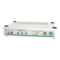
5 PICOSCALE HARDWARE
5.3.3 BOB analog GPIOs
The Breakout-Box buffers and normalizes the analog GPIOs to single ended signals with an ampli-
tude of ±10 V.
At the input ADC1 the single ended ±10 V signal is converted to a differential signal with an ampli-
tude equivalent to a full scale modulation of the ADC. Due to component tolerances, offsets and
gains can vary slightly so that ±10 V is not exactly equivalent to the ADC’s resolution. For an ex-
act mapping of voltage to ADC resolution it is recommended to do a calibration of the ADC input.
The input impedance of the ADC1 input is approx. 2.4 kΩ. The inputs ADC2 and ADC3 input are
converted a differential signal. Again, it is recommended to do a calibration to get an exact map-
ping from voltage to ADC resolution. The input impedance is approx. 34 kΩ. For a performance
overview see table 5.5 and 5.6.
Table 5.5: Main performance data of ADC1
Parameter Typical Value Unit
Full-scale input voltage ±10 V
Sample-rate 10 MS /s
Resolution 16 Bit
Bandwidth f
1dB
2-2.5 MHz
Table 5.6: Main performance data of ADC2 and ADC3
Parameter Typical Value Unit
Full-scale input voltage ±10 V
Sample-rate 100 kS /s
Resolution 16 Bit
Bandwidth f
1dB
35-45 kHz
The Breakout-Box converts the differential DAC1 signal from the PICOSCALE Controller to a single
ended ±10 V output signal. The output can drive currents up to 35 mA and a capacitive load up to
33 pF. DAC2-DAC5 are the PICOSCALE DAC signals normalized to ±10 V. If a single DAC channel
is connected, it can drive currents up to ±30 mA and a capacitive load of up to 200 pF. With more
channels connected, the maximum current reduces correspondingly. For a performance overview
see table 5.7 and 5.8.
39
PicoScale User Manual