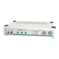
5 PICOSCALE HARDWARE
the lower part shows the options of the data line.
• (CPOL 0): The CLOCK LINE has a negative zero level .
• (CPOL 1): The CLOCK LINE has a positive zero level.
• (CPHA 0): The DATA LINE is written with the beginning of each clock cycle.
• (CPHA 1): The DATA LINE is written at the center of each clock cycle.
Furthermore, you can choose the data idle polarity.
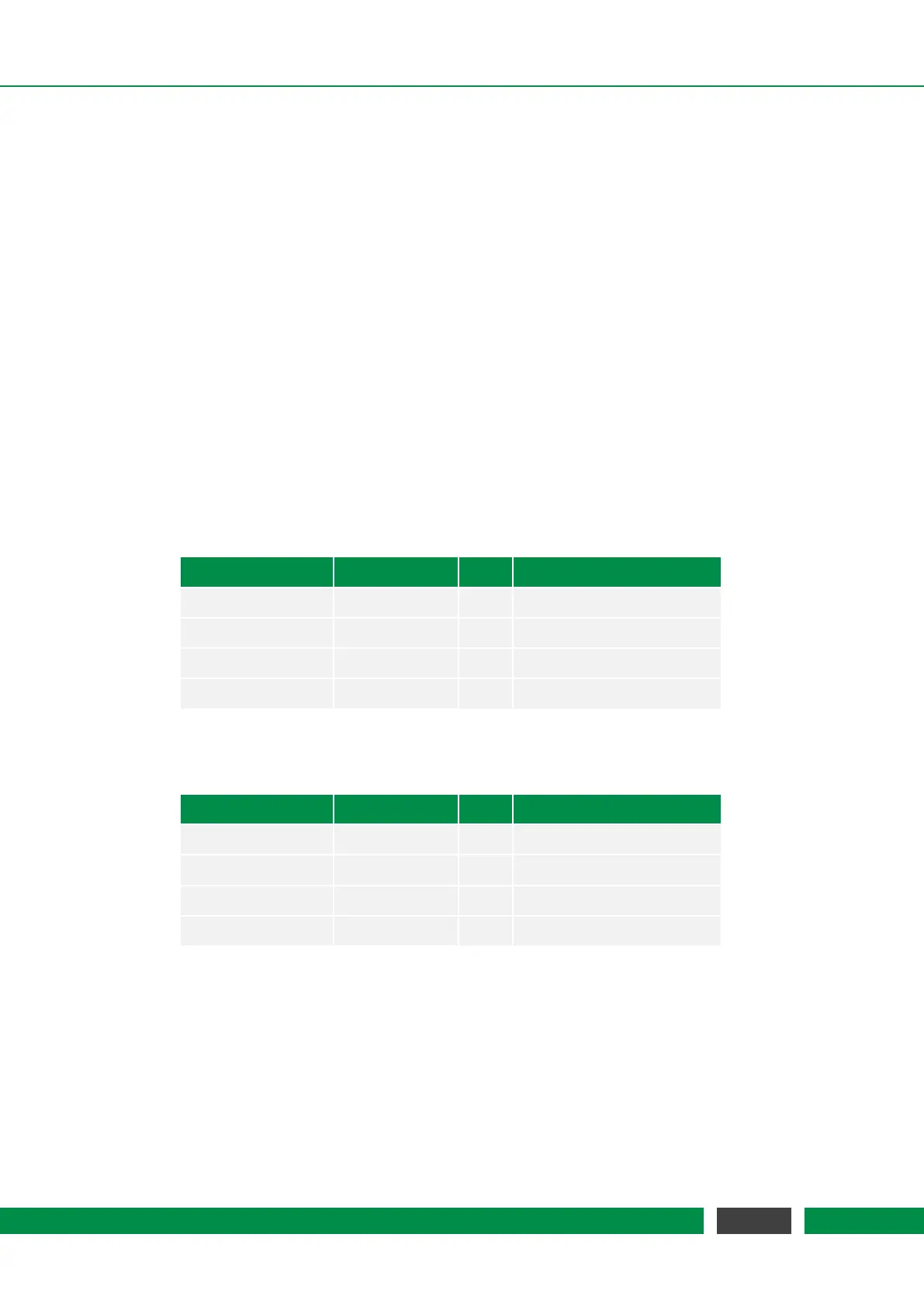
5.3.2 BOB digital GPIOs
The digital GPIOs are buffered on the Breakout-Box. The signals labelled with Digital1 - Digital4
have a 5 V high level, while the Digital5-Digital9 signals have a 3.3 V high level. All digital GPIOs
are matched with a 50 Ω serial resistor. The direction of the buffers is automatically set with the
direction of the digital GPIOs within the
PICOSCALE Controller. Main performance parameters
are listed in table 5.3 (for the Digital 1-4 signals) and table 5.4 (for the Digital 5-9 signals).
Table 5.3: Main performance data BOB Digital 1-4 GPIO Buffer
Parameter Typical Value Unit Comment
V
O
0 - 5 V Digital 1-4 output voltage
V
IH
3.5 V High-level input voltage
V
IL
1.5 V Low-level input voltage
rising/falling edge ≦ 50 ns
Table 5.4: Main performance data BOB Digital 5-9 GPIO Buffer
Parameter Typical Value Unit Comment
V
O
0 - 3.3 V Digital 5-9 output voltage
V
IH
2 V High-level input voltage
V
IL
0.8 V Low-level input voltage
rising/falling edge ≦ 50 ns
Due to the limited bandwidth it is recommended to use the digital GPIOs with a maximum fre-
quency of 1 MHz. Using higher frequencies may cause asymmetries in the duty cycle of the signal.
Depending on the cable connected to the BNC connector the digital GPIOs can over-/undershoot
with up to 1 V. The best signal form can be achieved in a 50 Ω environment and with short connec-
tions.
38
PicoScale User Manual