58
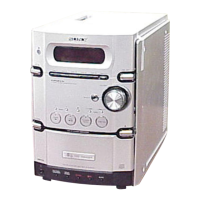
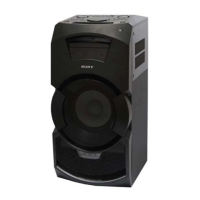
HCD-HPX7
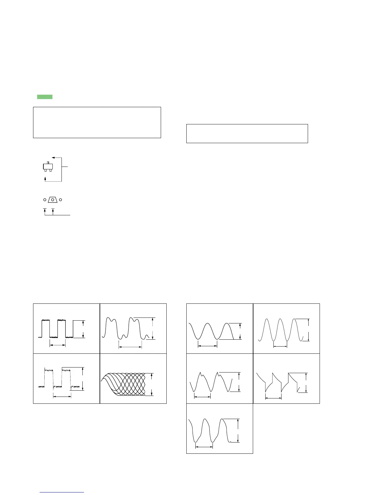
•Waveforms
Note on Schematic Diagram:
• All capacitors are in µF unless otherwise noted. (p: pF)
50 WV or less are not indicated except for electrolytics and
tantalums.
• All resistors are in Ω and
1
/
4
W or less unless otherwise
specified.
• f : internal component.
• 2 : nonflammable resistor.
• 5 : fusible resistor.
• C : panel designation.
• A : B+ Line.
• B : B– Line.
•Voltages and waveforms are dc with respect to ground un-
der no-signal conditions.
•Voltages are taken with a VOM (Input impedance 10 MΩ).
Voltage variations may be noted due to normal production
tolerances.
•Waveforms are taken with a oscilloscope.
Voltage variations may be noted due to normal production
tolerances.
• Circled numbers refer to waveforms.
• Signal path.
F : TUNER (FM/AM)
E : TAPE PLAY
a : TAPE REC
J : CD PLAY
L : AUX IN
•Abbreviation
AUS: Australian model
CND : Canadian model
E3 : 240 V AC area in E model
KR : Korean model
MX : Mexican model
TW : Taiwan model
NOTE FOR PRINTED WIRING BOARDS AND SCHEMATIC DIAGRAMS
Note on Printed Wiring Boards:
• X : parts extracted from the component side.
• Y : parts extracted from the conductor side.
• W : indicates side identified with part number.
• f : internal component.
• : Pattern from the side which enables seeing.
(The other layers' patterns are not indicated.)
Caution:
Pattern face side: Parts on the pattern face side seen from
(Conductor Side) the pattern face are indicated.
Parts face side: Parts on the parts face side seen from
(Component Side) the parts face are indicated.
C
B
These are omitted.
E
Q
B
These are omitted.
CE
Q
• Indication of transistor.
Note: The components identified by mark 0 or dotted
line with mark 0 are critical for safety.
Replace only with part number specified.
4.4 Vp-p
22.8
µ
s
4.5 Vp-p
472 ns
Approx.
700 mVp-p
4.5 Vp-p
59 ns
1
IC101 yd (LRCK)
2
IC101 yh (BCK)
– CD Board – – MAIN Board –
12.4 Vp-p
21.2
µ
s
2.6 Vp-p
21.2
µ
s
3.2 Vp-p
30.4
µ
s
2 Vp-p
62.6 ns
6.3 Vp-p
2 s
1
Q303, 304 (Collector)
(REC Mode)
2
Q303, 304 (Base)
(REC Mode)
3
IC306 qa (XCOUT)
4
IC306 qd (XOUT)
5
IC306 of (TC END SW)
(Tape Play Mode)
3
IC101 uj (XTAO)
4
IC101 ra (PFACO)