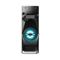
MAP-S1
84
Pin No. Pin Name I/O Description
115 UART_TxD_DEBUG O Serial data output terminal for fl ash writing Not used
116 DGND - Ground terminal
117 UART_RxD_DEBUG I Serial data input terminal for fl ash writing Not used
118 LED_GREEN O LED drive signal output terminal for the standby indicator “L”: LED on
119 D1.18V_SOC - Power supply terminal (+1.18V)
120 DAMP_SHUTDOWN O Shutdown control signal output to the digital power amplifi er “H”: shutdown
121 DGND - Ground terminal
122 DAMP_PROTECT I
Fault signal input from the digital power amplifi er “L”: fault
Speaker protect detection signal input terminal “L”: protect
123 D3.3V_SOC - Power supply terminal (+3.3V)
124 LINEOUT_MUTE O Line out and headphone muting on/off control signal output terminal “L”: muting on
125 I2C_SCL_CP I/O Two-way I2C clock signal bus with the MFI
126 I2C_SDA_CP I/O Two-way I2C data bus with the MFI
127 I2C_SCL_TU I/O Two-way I2C clock signal bus with the TUNER board
128 I2C_SDA_TU I/O Two-way I2C data bus with the TUNER board
129 I2C_SCL_IOEX O I2C clock signal output to the I/O expander
130 I2C_SDA_IOEX I/O Two-way I2C data bus with the I/O expander
131 PLL_UNLOCK I Unlock signal input from the clock multiplier
132 UART_RxD_BT I Serial data input from the Bluetooth module
133 EVOL_CLK O Serial data transfer clock signal output to the electrical volume
134 DAB1.2V P-ON O
Power on/off control signal output to the DAB board “H”: power on
(AEP, UK, Australian, Hong Kong and Malaysia models only)
135 SIRCS_IN I SIRCS signal input from remote control receiver
136 LED_RED O LED drive signal output terminal for the power on indicator “L”: LED on
137 AC_CUT I AC cut on/off detection signal input terminal “L”: AC cut on
138 DGND - Ground terminal
139 USB_X1 I System clock input terminal (48 MHz)
140 USB_X2 O System clock output terminal (48 MHz)
141 D3.3V_SOC - Power supply terminal (+3.3V)
142 DGND - Ground terminal
143 USB_DM (REAR) I/O Two-way USB data (–) bus with the USB (rear) connector
144 USB_DP (REAR) I/O Two-way USB data (+) bus with the USB (rear) connector
145 USB_VBUS (REAR) I VBUS power input terminal (for USB (rear))
146 D1.18V_SOC - Power supply terminal (+1.18V)
147 DGND - Ground terminal
148 D3.3V_SOC - Power supply terminal (+3.3V)
149 DGND - Ground terminal
150 USB0_DM I/O Two-way USB data (–) bus terminal Not used
151 USB0_DP I/O Two-way USB data (+) bus terminal Not used
152 USB0_VBUSIN I VBUS power input terminal Not used
153 D1.18V_SOC - Power supply terminal (+1.18V)
154 DGND - Ground terminal
155 REFRIN I Reference voltage input terminal Not used
156 DGND - Ground terminal
157 D3.3V_SOC - Power supply terminal (+3.3V)
158 D1.18V_SOC - Power supply terminal (+1.18V)
159 DGND - Ground terminal
160 D1.18V_SOC - Power supply terminal (+1.18V)
161 to
163
DGND - Ground terminal
164 FAN_SPEED O Fan motor speed control signal output terminal
165 USB_SW1 O USB data selection signal output terminal
166 QSPI_D2 O Write select signal output to the serial fl ash
167 QSPI_D3 O Hold signal output to the serial fl ash
168 QSPI_CLK O Serial data transfer clock signal output to the serial fl ash
169 QSPI_CS O Chip select signal output to the serial fl ash
170 QSPI_D0 O Serial data output to the serial fl ash
171 DGND - Ground terminal
172 QSPI_D1 I Serial data input from the serial fl ash
173 AC_RELAY O Relay drive signal output terminal (for main power)