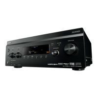
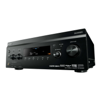
STR-DA2800ES
135
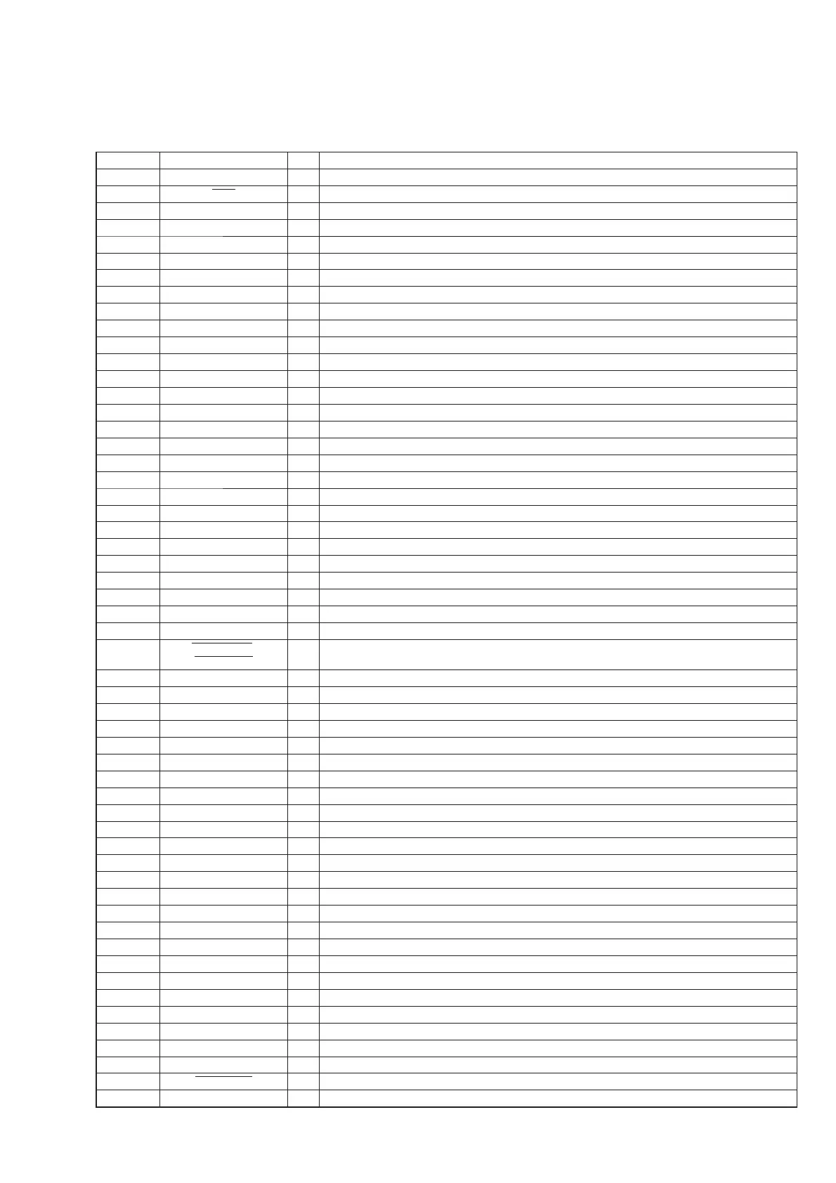
Pin No. Pin Name I/O Description
1 SDDQM O Data mask signal output to the SD-RAM
2 MS0
O Memory selection signal output to the SD-RAM
3 SDCKE O Clock enable signal output to the SD-RAM
4 VDD_INT - Power supply terminal (+1.2V) (for core)
5 CLK_CFG1 I Clock frequency setting terminal Fixed at “L” in this unit
6 ADDR0 O Address signal output to the SD-RAM
7 BOOT_CFG0 I Boot mode selection signal input terminal Fixed at “H” in this unit
8 VDD_EXT - Power supply terminal (+3.3V) (for I/O)
9 to 13 ADDR1 to ADDR5 O Address signal output to the SD-RAM
14 BOOT_CFG1 I Serial data input from the main system controller
15 GND - Ground terminal
16, 17 ADDR6, ADDR7 O Address signal output to the SD-RAM
18, 19 NC - Not used
20, 21 ADDR8, ADDR9 O Address signal output to the SD-RAM
22 CLK_CFG0 I Clock frequency setting terminal Fixed at “L” in this unit
23 VDD_INT - Power supply terminal (+1.2V) (for core)
24 CLKIN I System clock input terminal (25 MHz)
25 XTAL2 O System clock output terminal (25 MHz)
26 ADDR10 O Address signal output terminal Not used
27 SDA10 O Address signal output to the SD-RAM
28 VDD_EXT - Power supply terminal (+3.3V) (for I/O)
29 VDD_INT - Power supply terminal (+1.2V) (for core)
30 ADDR11 O Address signal output to the SD-RAM
31 ADDR12 O Address signal output terminal Not used
32 ADDR17 O Bank address signal output to the SD-RAM
33 ADDR13 O Address signal output terminal Not used
34 VDD_INT - Power supply terminal (+1.2V) (for core)
35 ADDR18 O Bank address signal output to the SD-RAM
36
RESETOUT
/
RUNRSTIN
I/O Reset signal output terminal/Running reset signal input terminal Not used
37 VDD_INT - Power supply terminal (+1.2V) (for core)
38 MOSI I Serial data input from the main system controller
39 MISO O Serial data output to the main system controller
40 SPICLK I Serial data transfer clock signal input from the main system controller
41 VDD_INT - Power supply terminal (+1.2V) (for core)
42 DPI_P05 I Chip select signal input from the main system controller
43 DSP_CS I Chip select signal input from the main system controller
44 MD - Not used
45 VDD_EXT - Power supply terminal (+3.3V) (for I/O)
46 NC - Not used
47 RESET_MAIN I Reset signal input terminal Not used
48 VDD_INT - Power supply terminal (+1.2V) (for core)
49 UART_OUT O Serial data output terminal Not used
50 UART_IN I Serial data input terminal Not used
51 LED O Not used
52 to 56 NC - Not used
57 VDD_EXT - Power supply terminal (+3.3V) (for I/O)
58 to 61 NC - Not used
62 VDD_INT - Power supply terminal (+1.2V) (for core)
63, 64 NC - Not used
65 VDD_INT - Power supply terminal (+1.2V) (for core)
66, 67 NC - Not used
68 VDD_INT - Power supply terminal (+1.2V) (for core)
69 NC - Not used
70 WDTRSTO
O Watchdog timer reset output terminal Not used
71 NC - Not used
• IC Pin Function Description
DSP BOARD IC5001 ADSST-AVR-3011 (DSP)