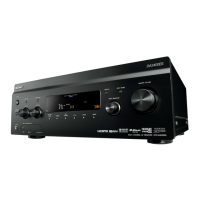
STR-DA2800ES
158
Pin No. Pin Name I/O Description
N8 DVCC33_IO - Power supply terminal (+3.3V)
N9 DGND - Ground terminal
N10 DVCC10_K - Power supply terminal (+1.1V)
N11 to
N17
DGND - Ground terminal
N18 DVCC10_K - Power supply terminal (+1.1V)
N19 DGND - Ground terminal
N21 DGND - Ground terminal
N23, N24 RDQ14_B, RDQ15_B I/O Two-way data bus with the SD-RAM
N25 DGND - Ground terminal
N26 to
N28
RDQ12_B, RDQ7_B,
RDQ6_B
I/O Two-way data bus with the SD-RAM
P1 FEFMO3 O Stepping motor drive signal output terminal Not used
P2, P3
FEMPXOUT1,
FEMPXOUT3
O Monitoring signal output terminal Not used
P4 FEGAINSW2 O Gain control signal output terminal Not used
P5 FECFREQ - Not used
P6 FEGAINSW3 O Gain control signal output terminal Not used
P8 DVCC33_IO - Power supply terminal (+3.3V)
P10 DGND - Ground terminal
P11 DVCC10_K - Power supply terminal (+1.1V)
P12 to
P18
DGND - Ground terminal
P19 DVCC10_K - Power supply terminal (+1.1V)
P21 DVCC15_IO_1 - Power supply terminal (+1.5V)
P23, P24 RDQ8_B, RDQ13_B I/O Two-way data bus with the SD-RAM
P25 RDQM0_B O Data mask signal output to the SD-RAM
P26 DVCC15_IO_1 - Power supply terminal (+1.5V)
P27 RDQS1_B_ O Data strobe signal (negative) output to the SD-RAM
P28 RDQS1_B O Data strobe signal (positive) output to the SD-RAM
R3 FECMOD - Not used
R4 REIC_MUTE1 O Motor drive muting control signal output terminal Not used
R5 FEOSCEN - Not used
R6 REIC_MUTE2 O Motor drive muting control signal output terminal Not used
R10 DVCC10_K - Power supply terminal (+1.1V)
R11 to
R17
DGND - Ground terminal
R18 DVCC10_K - Power supply terminal (+1.1V)
R19 DGND - Ground terminal
R21 DGND - Ground terminal
R23 RVREF_4 I Reference voltage (+0.75V) input terminal for SD-RAM
R24 RDQM1_B O Data mask signal output to the SD-RAM
R25 DVCC15_IO_1 - Power supply terminal (+1.5V)
R26 DGND - Ground terminal
R27 RDQS0_B O Data strobe signal (positive) output to the SD-RAM
R28 RDQS0_B_ O Data strobe signal (negative) output to the SD-RAM
T1 FEGAINSW1 O Gain control signal output terminal Not used
T2 to T5
FEGIO2, FEGIO4,
FEGIO8, FEGIO13,
FEGIO3
- Not used
T8 DVCC33_IO - Power supply terminal (+3.3V)
T10 DGND - Ground terminal
T11 DVCC10_K - Power supply terminal (+1.1V)
T12 to
T18
DGND - Ground terminal
T19 DVCC10_K - Power supply terminal (+1.1V)
T21 DVCC15_IO_1 - Power supply terminal (+1.5V)
T23 RDQ11_B I/O Two-way data bus with the SD-RAM
T24 RBA1_B O Bank address signal output to the SD-RAM
T25 to
T28
RDQ0_B, RDQ1_B,
RDQ10_B, RDQ9_B
I/O Two-way data bus with the SD-RAM