STR-DA2800ES
159
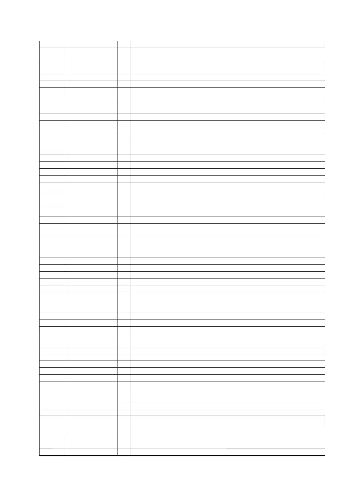
Pin No. Pin Name I/O Description
U1 to U3
FEGIO5, FEGIO6,
FEGIO10
- Not used
U4 FEEJECT_ I Disc eject detection signal input terminal Not used
U5, U6 FEGIO11, FEGIO12 - Not used
U9 DGND - Ground terminal
U10 DVCC10_K - Power supply terminal (+1.1V)
U11 to
U17
DGND - Ground terminal
U18 DVCC10_K - Power supply terminal (+1.1V)
U19 DGND - Ground terminal
U21 DGND - Ground terminal
U23, U24 RA12_B, RA1_B O Address signal output to the SD-RAM
U25, U26 RDQ3_B, RDQ2_B I/O Two-way data bus with the SD-RAM
V3 FEGIO9 - Not used
V4 FELIMIT_ I Sledge inner limit detection signal input terminal Not used
V5 FETRAYOUT_ I Disc tray in detection signal input terminal Not used
V6 REIC_TRAYIN# I Disc tray out detection signal input terminal Not used
V9 DVCC10_K - Power supply terminal (+1.1V)
V10 DGND - Ground terminal
V11 DVCC10_K - Power supply terminal (+1.1V)
V12 DGND - Ground terminal
V13 DVCC10_K - Power supply terminal (+1.1V)
V14 DGND - Ground terminal
V15 DVCC10_K - Power supply terminal (+1.1V)
V16 DGND - Ground terminal
V17 DVCC10_K - Power supply terminal (+1.1V)
V18 DGND - Ground terminal
V19 DVCC10_K - Power supply terminal (+1.1V)
V21 DVCC15_IO_1 - Power supply terminal (+1.5V)
V23, V24 RA11_B, RA4_B O Address signal output to the SD-RAM
V25 DGND - Ground terminal
V26 DVCC15_IO_1 - Power supply terminal (+1.5V)
V27 RCKE_B O Clock enable signal output to the SD-RAM
V28 RA10_B O Address signal output to the SD-RAM
W1 STXP O Transmit data (positive) output terminal Not used
W2 STXN O Transmit data (negative) output terminal Not used
W3 FEGIO7 - Not used
W4 FEPLAY_ I Disc play detection signal input terminal Not used
W5 REIC_FG I Motor hole sensor signal input terminal Not used
W6 AVSS12_SATA1 - Ground terminal
W9 DGND - Ground terminal
W10 DVCC10_K - Power supply terminal (+1.1V)
W11 DGND - Ground terminal
W12 DVCC10_K - Power supply terminal (+1.1V)
W13 DGND - Ground terminal
W14 DVCC10_K - Power supply terminal (+1.1V)
W15 DGND - Ground terminal
W16 DVCC10_K - Power supply terminal (+1.1V)
W17 DGND - Ground terminal
W18 DVCC10_K - Power supply terminal (+1.1V)
W19 DGND - Ground terminal
W21 DGND - Ground terminal
W24 RA6_B O Address signal output to the SD-RAM
W25 RBA2_B O Bank address signal output to the SD-RAM
W26 to
W28
RA9_B, RA7_B,
RA2_B
O Address signal output to the SD-RAM
Y1 SRXN I Receive data (negative) input terminal Not used
Y2 SRXP I Receive data (positive) input terminal Not used
Y3 AVDD12_SATA1 - Power supply terminal (+1.2V)
Y4 SREXT - External reference resistor connection terminal Not used