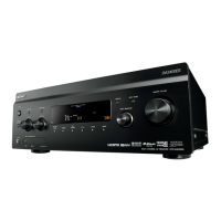
STR-DA2800ES
161
Pin No. Pin Name I/O Description
AD3 USB_2P_VRT - External reference resistor connection terminal
AD4 NFREN O Read enable signal output to the NAND fl ash
AD5 NFCEN2 O Chip enable signal output terminal Not used
AD6 GPIO4 O Jig mode selection signal output terminal
AD7 TCK I Test clock signal input terminal (for JTAG)
AD8 TDI I Test data input terminal (for JTAG)
AD9,
AD10
RDQM3, RDQM2 O Data mask signal output to the SD-RAM
AD12 RDQ23 I/O Two-way data bus with the SD-RAM
AD13 RA0 O Address signal output to the SD-RAM
AD14 RCAS_ O Column address signal output to the SD-RAM
AD15 to
AD18
RA5, RA13,
RA11, RA4
O Address signal output to the SD-RAM
AD19 RBA1 O Bank address signal output to the SD-RAM
AD20 RDQ11 I/O Two-way data bus with the SD-RAM
AD21 RDQM1 O Data mask signal output to the SD-RAM
AD22 RDQ14 I/O Two-way data bus with the SD-RAM
AD23 AVSS12_MEMPLL - Ground terminal
AD24,
AD25
RDQ29_B, RDQ24_B I/O Two-way data bus with the SD-RAM
AD26 RDQM2_B O Data mask signal output to the SD-RAM
AD27 RODT_B O On die termination enable signal output to the SD-RAM
AD28 RRAS_B O Row address signal output to the SD-RAM
AE1,
AE2
NFD7, NFD6 I/O Two-way data bus with the NAND fl ash
AE3 NFRBN O Ready/busy selection signal output to the NAND fl ash “L”: busy, “H”: ready
AE4 NFRBN2 O Ready/busy selection signal output terminal Not used
AE5 GPIO6 O Writing end fl ag signal output to the sub system controller “H”: end
AE6 GPIO5 I
Jig mode selection signal input from the main system controller
“L”: USB writing mode, “H”: normal mode
AE7 TMS I Test mode selection signal input terminal (for JTAG)
AE8,
AE9
RDQ24, RDQ26 I/O Two-way data bus with the SD-RAM
AE10 DVCC15_IO_1 - Power supply terminal (+1.5V)
AE11,
AE12
RDQ31, RDQ21 I/O Two-way data bus with the SD-RAM
AE13 RWE_ O Write enable signal output to the SD-RAM
AE14 DGND - Ground terminal
AE15 RCS_ O Chip select signal output to the SD-RAM
AE16 RA7 O Address signal output to the SD-RAM
AE17 DVCC15_IO_1 - Power supply terminal (+1.5V)
AE18 RDQ2 I/O Two-way data bus with the SD-RAM
AE19 RA1 O Address signal output to the SD-RAM
AE20 DGND - Ground terminal
AE21 RDQM0 O Data mask signal output to the SD-RAM
AE22 RDQ12 I/O Two-way data bus with the SD-RAM
AE23 AVDD12_MEMPLL - Power supply terminal (+1.2V)
AE24 TP_MEMPLL - Test terminal
AE25 RDQ25_B I/O Two-way data bus with the SD-RAM
AE26 RDQM3_B O Data mask signal output to the SD-RAM
AE27 RA0_B O Address signal output to the SD-RAM
AE28 RWE_B_ O Write enable signal output to the SD-RAM
AF1 to
AF3
NFD5, NFD4, NFD2 I/O Two-way data bus with the NAND fl ash
AF4 NFALE O Address latch enable signal output to the NAND fl ash
AF5 SFCK O Serial data transfer clock signal output terminal Not used
AF6 TDO O Test data output terminal (for JTAG)
AF7 TRST_ I Test reset signal input terminal (for JTAG)
AF8, AF9 RDQ25, RDQ27 I/O Two-way data bus with the SD-RAM
AF10 DGND - Ground terminal