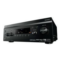
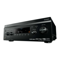
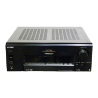
STR-DA2800ES
162
Pin No. Pin Name I/O Description
AF11,
AF12
RDQ30, RDQ20 I/O Two-way data bus with the SD-RAM
AF13,
AF14
DVCC15_IO_1 - Power supply terminal (+1.5V)
AF15,
AF16
RA9, RA2 O Address signal output to the SD-RAM
AF17 DGND - Ground terminal
AF18,
AF19
RDQ1, RDQ3 I/O Two-way data bus with the SD-RAM
AF20 DVCC15_IO_1 - Power supply terminal (+1.5V)
AF21 to
AF23
RDQ15, RDQ6,
RDQ5
I/O Two-way data bus with the SD-RAM
AF24 TN_MEMPLL - Test terminal
AF25 RDQ16_B I/O Two-way data bus with the SD-RAM
AF26 DGND - Ground terminal
AF27 RDQS3_B_ O Data strobe signal (negative) output to the SD-RAM
AF28 RDQS3_B O Data strobe signal (positive) output to the SD-RAM
AG1,
AG2
NFD3, NFD0 I/O Two-way data bus with the NAND fl ash
AG3 NFCLE O Command latch enable signal output to the NAND fl ash
AG4 NFWEN O Write enable signal output to the NAND fl ash
AG5 SFDI I Interrupt signal input from the IR controller
AG7,
AG8
RDQ16, RDQ19 I/O Two-way data bus with the SD-RAM
AG9 RDQS2 O Data strobe signal (positive) output to the SD-RAM
AG10 RDQS3_ O Data strobe signal (negative) output to the SD-RAM
AG11 RDQ29 I/O Two-way data bus with the SD-RAM
AG13 RCLK1 O Clock signal (positive) output to the SD-RAM
AG14 RBA0 O Bank address signal output to the SD-RAM
AG16 RCKE O Clock enable signal output to the SD-RAM
AG17,
AG19
RDQ0, RDQ9 I/O Two-way data bus with the SD-RAM
AG20 RDQS0 O Data strobe signal (positive) output to the SD-RAM
AG21 RDQS1_ O Data strobe signal (negative) output to the SD-RAM
AG22 RDQ7 I/O Two-way data bus with the SD-RAM
AG24 RCLK0 O Clock signal (positive) output to the SD-RAM
AG25 RDQ17_B I/O Two-way data bus with the SD-RAM
AG26 DVCC15_IO_1 - Power supply terminal (+1.5V)
AG27 RDQS2_B O Data strobe signal (positive) output to the SD-RAM
AG28 RDQS2_B_ O Data strobe signal (negative) output to the SD-RAM
AH1 NFD1 I/O Two-way data bus with the NAND fl ash
AH2 NFCEN O Chip enable signal output to the NAND fl ash
AH4 SFDO O Serial data output terminal Not used
AH5 SFCS O Chip select signal output terminal Not used
AH7,
AH8
RDQ17, RDQ18 I/O Two-way data bus with the SD-RAM
AH9 RDQS2_ O Data strobe signal (negative) output to the SD-RAM
AH10 RDQS3 O Data strobe signal (positive) output to the SD-RAM
AH11 RDQ28 I/O Two-way data bus with the SD-RAM
AH13 RCLK1_ O Clock signal (negative) output to the SD-RAM
AH14 RA3 O Address signal output to the SD-RAM
AH16,
AH17
RA8, RA10 O Address signal output to the SD-RAM
AH19 RDQ8 I/O Two-way data bus with the SD-RAM
AH20 RDQS0_ O Data strobe signal (negative) output to the SD-RAM
AH21 RDQS1 O Data strobe signal (positive) output to the SD-RAM
AH22 RDQ13 I/O Two-way data bus with the SD-RAM
AH24 RCLK0_ O Clock signal (negative) output to the SD-RAM
AH25 to
AH28
RDQ18_B, RDQ19_B,
RDQ26_B, RDQ27_B
I/O Two-way data bus with the SD-RAM