General purpose and alternate function I/O (GPIO and AFIO) UM0306
74/519
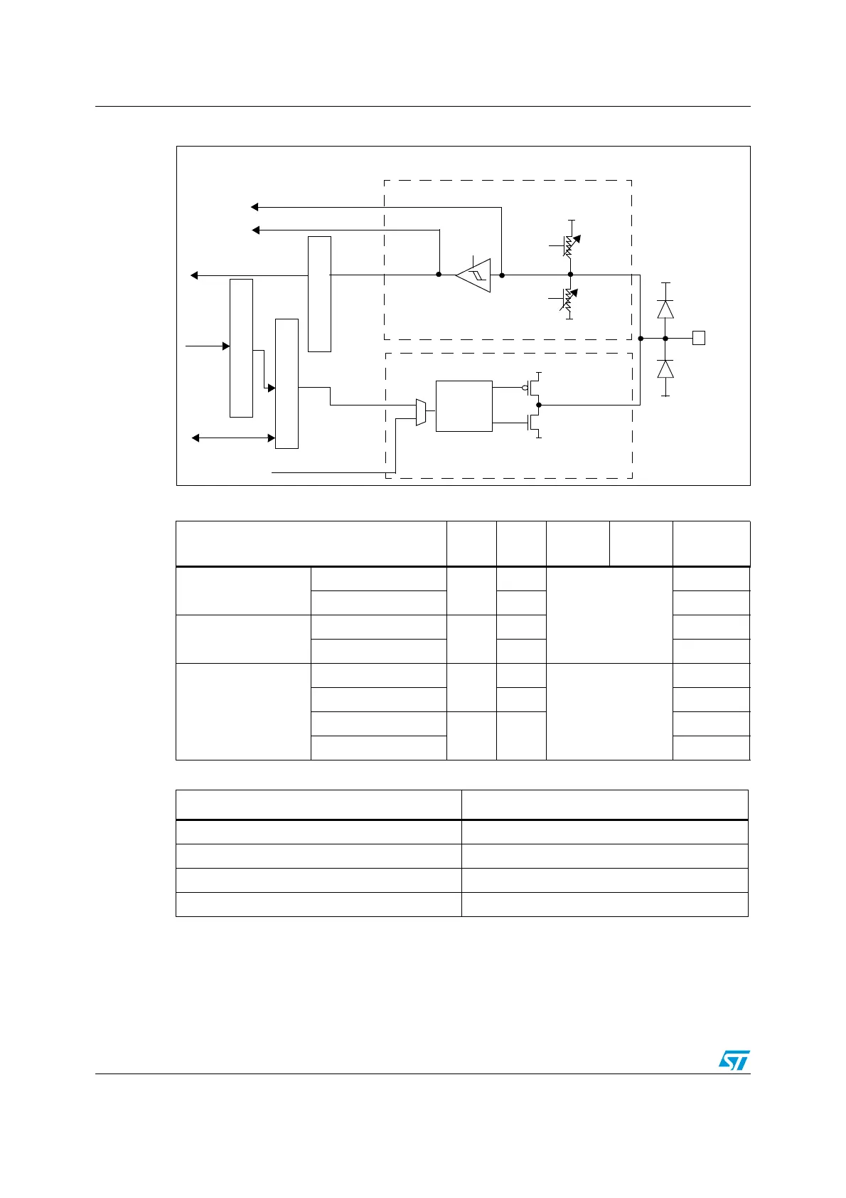
Figure 9. Basic structure of an I/O port bit
5.1.1 General purpose I/O (GPIO)
During and just after reset, the alternate functions are not active and the I/O ports are
configured in Input Floating mode (CNFx[1:0]=01b, MODE[1:0]=00b).
Table 11. Port bit configuration table
Configuration mode CNF1 CNF0 MODE1 MODE0
PxODR
Register
General purpose
output
Push-Pull
0
0
01
10
11
see Ta bl e 12
0 or 1
Open-Drain 1 0 or 1
Alternate Function
output
Push-Pull
1
0 don’t care
Open-Drain 1 don’t care
Input
Analog input
0
0
00
don’t care
Input Floating 1 don’t care
Input Pull-Down
10
0
Input Pull-Up 1
Table 12. Output Mode bits
MODE[1:0] Meaning
00 Reserved
01 Max. output speed 10 MHz
10 Max. output speed 2 MHz
11 Max. output speed 50 MHz
Alternate Function Output
Alternate Function Input
PUSH-PULL,
OPEN-DRAIN OR
DISABLED
INPUT DATA REGISTER
OUTPUT DATA REGISTER
READ/WRITE
FROM ON-CHIP
PERIPHERAL
TO ON-CHIP
PERIPHERAL
OUTPUT
CONTROL
Analog Input
ON/OFF
PULL
PULL
ON/OFF
I/O PIN
VDD_IO
VDD_IO
VSS
VSS
TTL SCHMITT
TRIGGER
VSS
VDD_IO
PROTECTION
DIODE
PROTECTION
DIODE
ON/OFF
INPUT DRIVER
OUTPUT DRIVER
DOWN
UP
P-MOS
N-MOS
READ
BIT SET/RESET REGISTERS
WRITE
 Loading...


