your position is our focus
LEA-LA LEA-4A / LEA -4S Remarks for Migration
Pin
PinName TypicalAssignment PinName TypicalAssignment
22 GPSMODE2
ConnectedtoGND
orVDD_18OUT
GPSMODE2/
GPSMODE23
25
Notconnected
Backwardcompatible:Thispincanbeconnected
toGND,VDD18OUTorVCC.Anexternalpullup
resistorisnotrequiredasthereisonebuilt-in.
23 NC
Notconnected
GPSMODE7
Notconnected
24 NC
ConnectedtoGND
VDDUSB
ConnectedtoGND
25 NC
Notconnected
USB_DM
Notconnected
26 NC
Notconnected
USB_DP
Notconnected
PlacingaLEA-4xintoanexistingLEA-LAboard
designwilldisableUSBport.
27 EXTINT0
Connectedto
VDD18OUT
EXTINT0
Notconnected
Donotaddanexternalpullupresistor;thereis
onebuilt-intoV_BAT.Leaveopenifnotused.
28 TIMEPULSE
1.8Vout
TIMEPULSE
VDDIOlevelI/O
ConsiderthatTIMPULSEonLEA-4xisonVDDIO
voltagelevel(1.8VonLEA-LA)
J:Pinstobecheckedcarefully
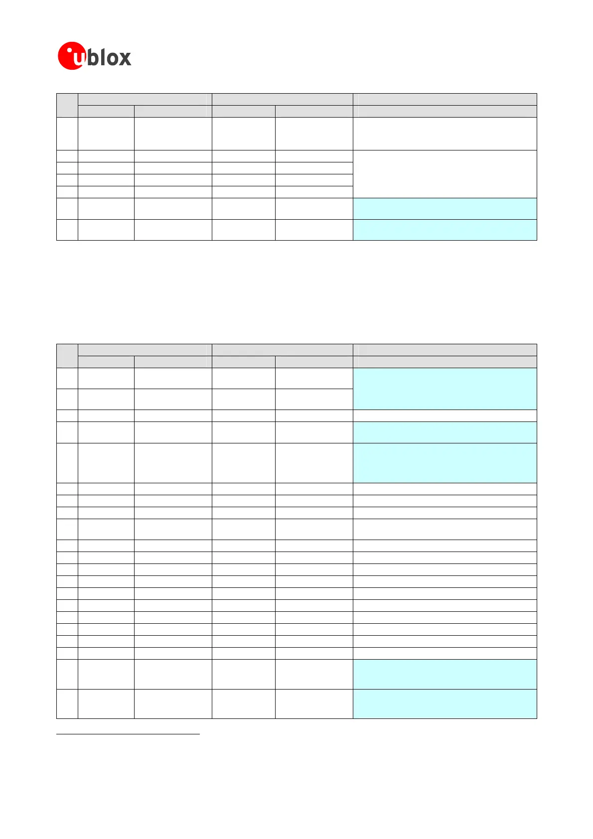
Table 79: Pin-out comparison LEA-LA vs. LEA-4A/4S
D.3 Migration from LEA-LA to LEA-4H/LEA-4P
The pin-outs of LEA-LA and LEA-4H/4P differ slightly. compares the modules and highlights the
differencestobeconsidered.
Table 80
LEA-LA LEA-4H / LEA-4P Remarks for Migration
Pin
PinName TypicalAssignment PinName TypicalAssignment
1 TXD2
VDDIOlevelI/O
MISO
VDDIOlevelI/O;
notconnected
2 RXD2
VDDIOlevelI/O;
pullupifnotused
MOSI
VDDIOlevelI/O;
notconnected
SerialPort2notsupportedonLEA-4P/LEA-4H.
Leaveopenifnotused.
3 TXD1
VDDIOlevelI/O
TXD1
VDDIOlevelI/O Nodifference
4 RXD1
VDDIOlevelI/O;
pullupifnotused
RXD1
VDDIOlevelI/O
Donotaddanexternalpullupresistor;thereis
onebuilt-intoV_BAT.Leaveopenifnotused.
5 VDDIO
1.65–3.60V
VDDIO
1.65–3.60V
TobecompatibletoLEA-LA,VDDIOhastobeset
toVcctoassurea3.0Vlevelattheserialports.
TheGPSMODEpinsdorecognize1.8Vand3.0V
as“high”valueatVDDIO.
6 VCC
2.70–3.30V
VCC
2.70–3.30V Nodifference
7 GND
GND
GND
GND Nodifference
8 VDD18OUT
Notconnected
VDD18OUT
Notconnected Nodifference
9 GPSMODE6
ConnectedtoGND
orVDD_18OUT
PCS0_N
Notconnected
Backwardcompatible:canbeleftopenor
connectedtoGND,VDDIOorVDD_18OUT.
10 RESET_N
1.8V
RESET_N
1.8V
Nodifference(seeSection4.9.2).
11 V_BAT
1.95–3.6V
V_BAT
1.50 Widervoltagerange.Uncriticalformigration.–3.6V
12 BOOT_INT
NC
BOOT_INT
NC Nodifference
13 GND
GND
GND
GND Nodifference
14 GND
GND
GND
GND Nodifference
15 G
fference
ND
GND
GND
GND Nodi
16 RF_IN
RF_IN
RF_IN
RF_IN Nodifference
17 GND
GND
GND
GND Nodifference
18 VCC_RF
VCC-0.1V
VCC_RF
VCC-0.1V Nodifference
19 V_ANT
3.0V–5.0V
V_ANT
3.0V-5.0V Nodifference
20 AADET_N
ConnectedtoGND
AADET_N
Notconnected
Noexternalpulldownresistorrequired,asthereis
alreadyaninternalpulldownresistor.Pleasecheck
resistorvaluesin Section 4.3.3.2.
21 GPSMODE5
ConnectedtoGND
orVDD_18OUT
EXTINT1
Notconnected
Donotaddanexternalpullupresistor;thereis
onebuilt-in.Leaveopenifnotused.If
ermanentl
connectedtoGND,theFixNOWslee
25
ConnectingtheGPSMODE23pin(LEA-4S)toGNDincreasedtheFixNOW sleepmodecurrentbyabout50µA.ConnectingtheGPSMODE2
pin(LEA-4A)toGNDdoeshowevernothaveanimpactontheFixNOWsleepmodecurrent.
GPSModules-SystemIntegrationManual(SIM)(incl.ReferenceDesign) MigrationtoANTARISP®P4receivers
GPS.G4-MS4-05007-A1
Page 168
 Loading...