your position is our focus
4 Receiver Description
4.1 Overview
TheANTARIS
®
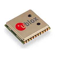
4GPSModule isa self-containedreceiverfor theGlobal PositioningSystem(GPS). Thecomplete
signalprocessingchainfromantennainputtoserialoutputiscontainedwithinasinglecomponent.
Theheightof3mm(~120mil)andsmallsizemakesittheidealGPSsolutionforapplicationswithstringentspace
requirements.This
typeofpackagemakesexpensiveRFcablingobsolete.TheRFinputisavailabledirectlyon a
pin,theANTARIS
®
4
GPSModuleisSMTsolderableandcanbehandledbystandardpickandplaceequipment.
The ANTARIS
®
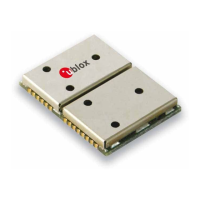
4 GPS Receiver provides up to two serial ports, which can handle NMEA, UBX proprietary data
formatanddifferentialGPScorrectiondata(RTCM)andaUSBdeviceport(onlyLEA-4xandNEO-4xmodules)
4.1.1 Block Schematic
TheANTARIS
®
4
GPSreceiverisdividedintotwo distinct,separatelyshielded sections. Thesmallersection isthe
RF-Section,thelargersectioncontainsthebaseband.
TheRFsectioncontainsthelownoiseamplifier(LNA)ATR0610,theSAWbandpassfilter,theRF-ICATR0601and
the GPS crystal. The ATR0601 uses a single IF sub-sampling
scheme with an analogue IF of 96.764MHz, a
samplingfrequencyof23.104MHz,andaresultingdigitalIFof4.348MHz.
The baseband section contains the digital circuitry comprised of the ATR062x baseband processor, the RTC
crystalandadditionalelementsassuchoptionalFLASHmemorywherespecified.
d by a number of digital signals: Control signals from the digital part switch
The two
sections are connecte
betweendifferentpowerstatesoftheRFsection.The23.104MHzclockissuppliedtothedigitalpartaswellas
the1.5bitquantizedIFsignal.Anotherstatussignalreportsthestatusofthe
antennabiasinputtothebaseband
processor.Finally,afterrigorousfiltering,powerissuppliedfromthedigitalparttotheRFpart.
ATR0601
ATR062x
Battery
backed
RAM (
BBR
)
4kB
[32 Bit]
RESET
ARM7
CPU
SRAM
128 kB
[32 Bit]
ROM
288 kB
[32 Bit]
GPS
Channels
FLASH
Memory
min.
4Mbit
[16 Bit]
32.768 kHz
Data Bus
Digital IF & Clock
1.8V
LDO
VBAT
LDO
RTC
23.104 MHz
I/Os
XTO
VCC
GND
Boot_int
RxD1
TxD1
TxD2
RxD2
R
V_ant
P0
RF_ON SLEEP_N
GND
SAW-Filter
A
D
I/Os
Address Bus
F_in
GND
AADET_N
VBAT
Reset_N (O.D. @ 1.8 V)
P15
ATR0610
(optional)
GPIO Pi
GPSMODE Pins
EXTINT0
ns or
USB
Figure 48: Hardware Block Schematic
GPSModules-SystemIntegrationManual(SIM)(incl.ReferenceDesign) ReceiverDescription
GPS.G4-MS4-05007-A1
Page 59
 Loading...