your position is our focus
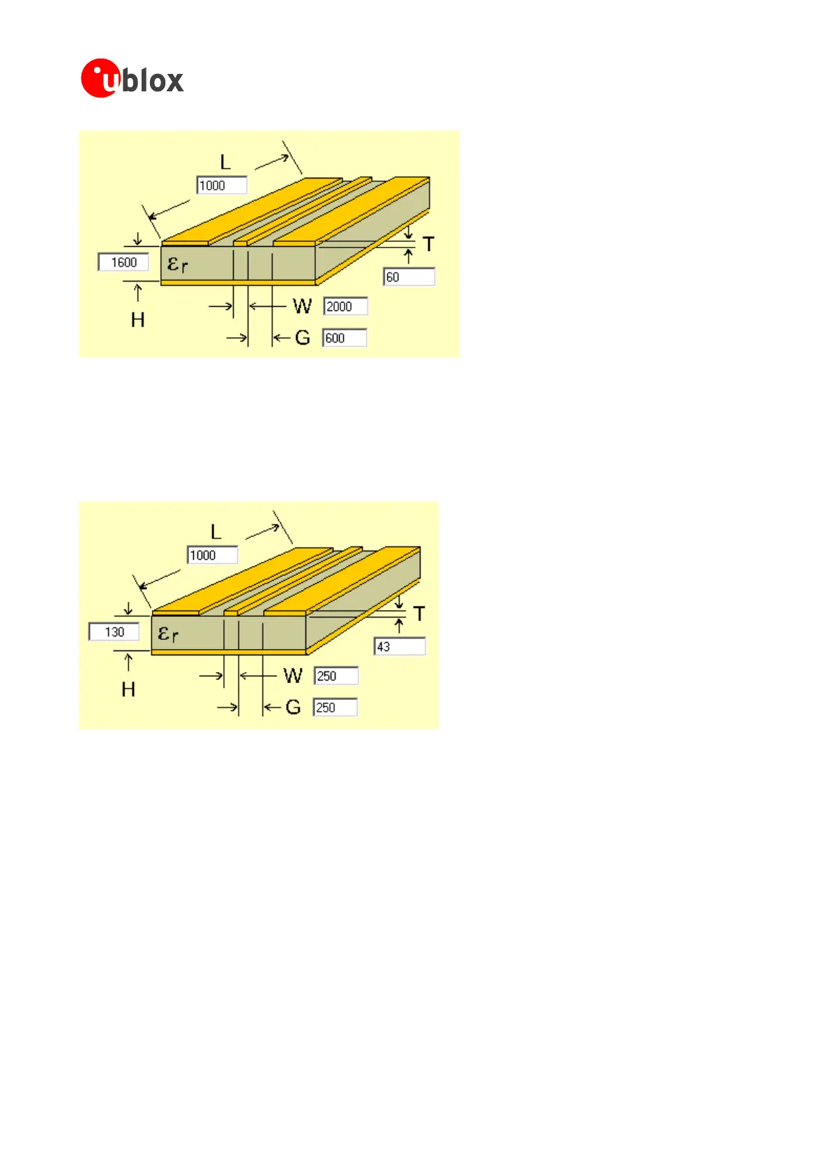
Figure 45: Micro strip on a 2-layer board (Agilent AppCAD Coplanar Waveguide)
ng (35µm) plus the plated cupper (typically 25µm).
Figure 45showsanexampleofa2-layerFR4boardof1.6mmthicknessanda35µm(1once)coppercladding.
The thickness of the micro strip is comprised of the claddi
Figure 46 depicts an example of a multi layer FR4 board with 18µm (½
once) cladding and 180µ dielectric
betweenlayer1and2.
Figure 46: Micro strip on a multi layer board (Agilent AppCAD Coplanar Waveguide)
3.6.6 Antenna Bias Voltage on NEO-4S and LEA-4M
NEO-4SandLEA-4MdonotprovidetheantennabiasvoltageforactiveantennasattheRF_INpin.Itistherefore
necessary to provide this voltage outside the module via an inductor as indicated in Figure 62. For optimal
performance,itisimportanttoplacetheinductorasclosetothemicrostrip
aspossible.Figure 47illustratesthe
recommendedlayoutandalsoshowsanexampleofhowitshouldnotbedone.
GPSModules-SystemIntegrationManual(SIM)(incl.ReferenceDesign) Design-In
GPS.G4-MS4-05007-A1
Page 57
 Loading...