your position is our focus
D.4 Migration
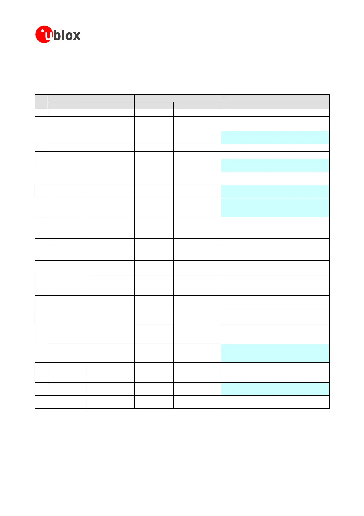
The pin-outs of TIM
from TIM-Lx to TIM-4x pin out
-Lx and TIM-4x modules do not differ significantly. Table 81 compares the modules and
ighlights the differences to be considered. Please note that this table does not consider any migration from
TIM-LR.
h
TIM-Lx TIM-4x Remarks
Pin
PinName TypicalAssignment PinName TypicalAssignment
1 VCC
2.70–3.30V
VCC
2.70–3.30V Nodifference
2 GND
GND
GND
GND renceNodiffe
3 BOOT_INT
NC
BOOT_INT
NC renceNodiffe
4 RXD1
3.0Vin;pullupto
VCCifnotused
RXD1
1.8-5.0Vin
Donotaddanexternalpullupresistor;thereis
onebuilt-intoV_BAT.Leaveopenifnotused.
5 TXD1
3.0Vout
TXD1
3.0Vout Nodifference
6 TXD2
3.0Vout
TXD2
3.0Vout Nodifference
7 RXD2
3.0Vin;pullupto
used
RXD2
1.8-5.
VCCifnot
0Vin
Donotaddanexternalpullupresistor;thereis
onebuilt-intoV_BAT.Leaveopenifnotused.
8
P17 /
GPSMODE5
1.8VI/O(LP:3.0V),
notconnected
P17/
GPSMODE5
3.0VI/O
connected
nce
26
,not
Nodiffere
9
GPSMOD
STATUS / 1.8VI/O(LP
E3
:3.0V),
notconnected
EXTINT1 /
GPSMODE3
3.0VI/O,
connecte
not
d
StatusPinnotavailableanymore;Nodifference
otherwise.
10
VDD18_OUT /
TIM-LP:
NC/GND
Notconnected
VDD18OUT
Notconnected
Nodifference,exceptforTIM-LP.
11
to
16
GND
GND
GND
GND Nodifference
17 RF_IN
RF_IN
RF_IN
RF_IN Nodifference
GND
GND
GND rence
18 GND
Nodiffe
3.0V-5.0V
V_ANT
3.0V-5.0 Nodifference
19 V_ANT
V
20 VCC_RF
VCC-0.1V
VCC_RF
VCC-0.1 NodifferenceV
21 V_BAT
1.95–3.6V
V_BAT
1.50– Uncriticalformigration.3.6V Widervoltagerange.
22 RESET_N
1.8V
RESET_N
1.8V
Nodifference.Don’tdrivehigh. Referto
Section 4.9.2 formoreinformation.
23 EXTINT0
Notconnected
EXTINT0
Notcon Nodifferencenected
PCS1_N/
GPSMODE2
difference
24
GPSMODE2
PCS1_N/
No
25
PCS0_N/
GPSMODE6
PCS0_N/
GPSMODE6
Nodifference
E7
1.8VI/O(LP:3.0V),
SCK/
NC
3.0VI/O,not
connected
NodifferenceonProgrammable receivers.
ButonTIM-4A:theNavigationratecannotbe
changedanymore.It’salways1Hz.
26
SCK/
GPSMOD
notconnected
Noexternalpulldownresistorrequiredasthere
27 AADET_N
Notconnected
AADET_N
Notconnected
isalreadyaninternalpulldownregister.Please
checkresistorvaluesinSection 4.3.3.2.
28
GPSMODE8
MOSI/ 1.8VI/O(LP:3.0V),
MO
notconnected
SI/
P24
3.0VI/O
connec
onProgrammablereceivers.
/TIM-4S:theNavigationrate
be danymore.It’salways1Hz.
,not
rence
ted
ButonTIM-4A
nnot change
Nodiffe
ca
1.8Vout
(LP:3.0V)
TIMEPULSE
3.0Vou
29 TIMEPULSE
t
Samefunctionbutdifferentoutputvoltage.
30
PCS3_N/
GPSMODE12
1.8VI/O(LP:3.0V),
notconnected
PCS3_N/
GPSMODE 12
3.0VI/O,not
connecte
Nodifference
d
J nstobecheckedcarefully
Pin-out comparison TIM-Lx vs. TIM-4x
:Pi
Table 81:
isonlysignificantwhenusingGPIOpinfunctionalitytogetherwithanSCKitapplication.
26
Higheroutputvoltage
GPSModules-SystemIntegrationManual(SIM)(incl.ReferenceDesign) MigrationtoANTARISP®P4receivers
GPS.G4-MS4-05007-A1
Page 170
 Loading...