your position is our focus
4.2 Power Management
4.2.1 Connecting Power
TheANTARIS
®
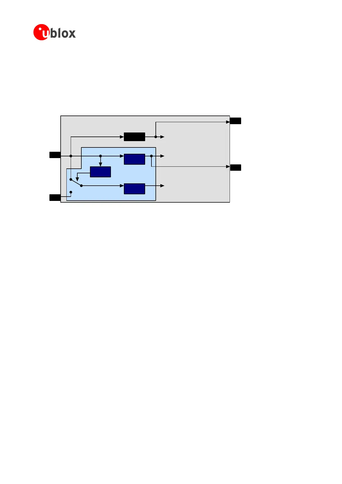
4GPSReceiverbasicallyhastwopowersupplypins,VCCandVBAT.ForLEAmodulesthereisan
additional pad power supply pin VDDIO that defines the IO voltage levels. Figure 50 shows the internal
connectionsofthepowersupplynetwork.
ANTARIS4 BasebandChip
VCC
VBAT
VCC
LDO
VBAT
LDO
Voltage
Super visor
1.8 V to ATR062x core,
FLASH
1.8 V to ATR0621 RTC
and backup SRAM
Noise F
to RF section:
A and ATR0601
ilter
LN
VCC_RF
VDD18OUT
Figure 50: Power supply concept
4.2.1.1 VCC - Main Power
Main power supply is fed through the VCC pin. During operation, the current drawn by the ANTARIS
®
4 GPS
me orders of magnitude, especially, if low-power operation modes are enabled. It is
important that the system power supply circuitry is able to support the peak power (see datasheet for
specification) for a short time. In order to dimension a battery capacity for certain application
the sustained
seofVCCripplevoltageatthemodule.Itisalsoagoodideatoplacea
In case failure on pin VCC,real-time clockandbackup RAM aresuppliedthrough pinV_bat.This
enables the ANTARIS
®
4 GPS receiver to recover from power failure with either a Hotstart or a Warmstart
(dependingontheduration ofVCC outage)andtomaintain theconfigurationsettings.If noBackupBatteryis
connected,thereceiverperformsaColdstartatpowerup.
Note Ifnobackupbatteryisavailableconnectthe
V_batpintoGND.
Receiver can vary by so
powerfigureshallbeused.
Note AGPSreceiverissensitivetoripplesonthepowersupplyvoltage.Themaxripplemustnotexceed50
mVpeaktopeak.Itisstronglyrecommendedtodesignalow-resistanceconnectionfromthevoltage
regulator to the VCC supply pin of
the module. Any resistive or inductive losses in this path may
resultinanundesiredincrea
largecapacitor,e.g.10µF,closetotheVCCpinofthemodule.
4.2.2 Backup Battery
powerof a
GPSModules-SystemIntegrationManual(SIM)(incl.ReferenceDesign) ReceiverDescription
GPS.G4-MS4-05007-A1
Page 61
 Loading...