your position is our focus
GND
RF_IN
GND
AADET_N/NC
15
16
17
18
19
28
27
26
25
24
23
22
21
20
14
13
12
11
10
1
2
3
4
5
6
7
8
9
VCC
TxD2
RxD2
RESET_N
VBAT
GND
RxD1
TxD1
BOOT_INT
GND
Vcc
Micro
cessorPro
(serial)
Passive Antenna
VCC_RF
V_ANT/NC
GPSMO
USB_DP
VDDUSB
USB_D
TIMEPULSE
EXTINT0
GND
VDDIO
DE5
M
VDD18OUT
LEA-
LEA-4S
GPSMODE2/
GPSMODE7
1)
4A / LEA-4M/
GPSMODE6
Backup
Battery
+
Micro
Processor
(USB)
1) USB selfpowered s g
(optional)
ettin
USB port
GND
RF_IN
GND
ET_NAAD
15
16
17
18
19
28
27
26
25
24
23
22
21
20
14
13
12
11
10
1
2
3
4
5
6
7
8
9
TxD1
RESET_N
BOOT_INT
GND
VCC
RxD1
MISO
MOSI
VBAT
GND
Vcc
Micro
Processor
(serial)
Passive Antenna
VCC_RF
V_ANT
EXTINT1/ P13
VDD18OUT
USB_DP
USB_DM
GND
VDDUSB
VDDIO
TIMEPULSE
EXTINT0/ P9
LEA-4P/ LEA-4H/
LEA-4T
PCS2_N/ P12
PCS0_N/ SS_N/ P26
SCK/ P23
Backup
Battery
+
Micro
Processor
(USB)
USB port (optional)
GPSMODE23
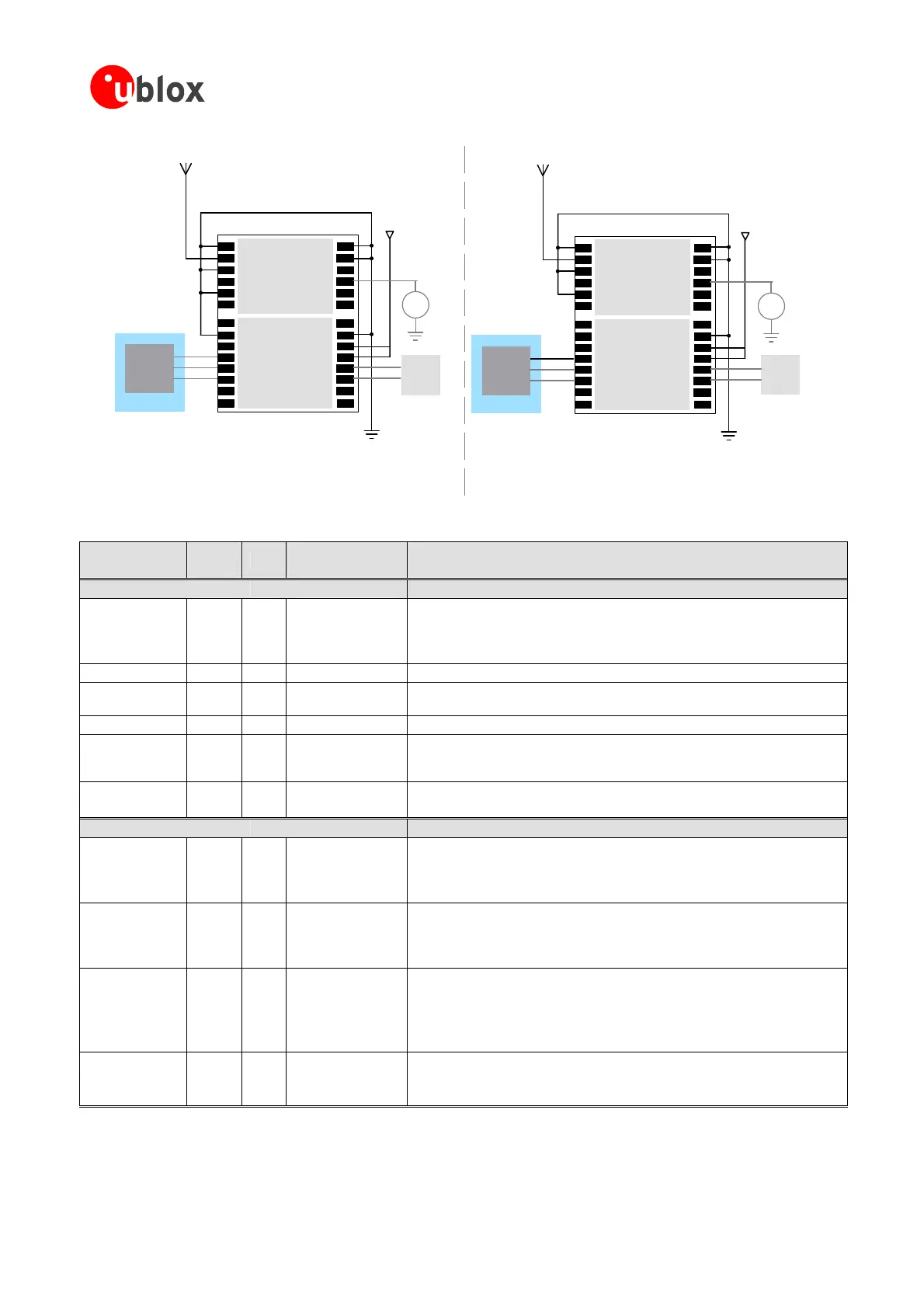
Figure 37: Passive Antenna Design ceivers for LEA-4x Re
Function
PIN
( LEA)
I/O Description Remarks
Power
VDDIO
5 I
Supplyvoltagefor
digitalI/Opins
pins(e.g.serialports,TIMEPULSE).Mustbe
etingdatasheet
PowerSupplyforthedigitalI/O
connectedtoVDD18OUT,VCCorothervoltageso urceme
specification.
ever leave open!N
VCC
6 I SupplyVoltage
50mVppMaxallowedrippleonVCC=
GND
7,13-
15,17
I Ground
allGNDpinsofthemodule,preferablywithAssureagoodGNDconnectionto
alargegroundplane(fordetailsrefertoSection 3.6.4)
VDD18OUT
8 O 1.8Vsupplyoutput
1.8Voutputvoltagereference.Leaveopenifnotused.
VBAT
11 I
Backupvoltage
supply
pbatterytoV_BATinorder toenable
onthereceivers.OtherwiseconnecttoGND.See
It’srecommendedtoconnectabacku
WarmandHotStartfeatures
alsoSection 4.2.2.
VDD_USB
24 I USBPowerSupply
TousetheUSBinterfaceconnectthispinto3.0–3.6V.SeealsoSection 4.4.2
IfnoUSBserialportusedconnecttoGND.
Antenna
RF_IN
16 I
fromantenna
eacontrolled
RF_INtotheantennaortheantenna
tion 3.6.5)
GPSsignalinput
TheconnectiontotheantennahastoberoutedonthePCB.Us
impedanceof50Ohmtoconnect
connector(fordetailsrefertoSec
Don’tsupplyDCthroughthispin.UseV_ANTpin
tosupplypower.
VCC_RF
18
OutputVoltageRF
section
oftheAntennamustnotexceedthe
themodule(seealso4.3.3).
O
Canbeusedtopoweranexternalactiveantenna(VCC_RFconnectedto
V_ANT).Themaxpowerconsumption
datasheetspecificationof
Leaveopenifnotused.
I
AntennaBias
voltage
GND
If Antenna
inputtotheAntennaBiasVoltageorVCC_RFforshortcircuitprotectionoruse
theantennasupervisorcircuitry(see 4.3.3.2).
This
pinisnotavailableonLEA-4M(seesection3.6.6formoreinformation).
Connectto ifPassiveAntennaisused.
anactive isused,adda10Rresistor(see 4.3.3.2)infrontofV_ANT
V_ANT
19
AADET_N
20 I
ActiveAntenna
Detect
Inputpinforoptionalantennasupervisorcircuitry(see 4.3.3.2).
Leaveopenifnotused.
ThispinisnotavailableonLEA-4M(seesection3.6.6formoreinformation).
GPSModules-SystemIntegrationManual(SIM)(incl.ReferenceDesign) Design-In
GPS.G4-MS4-05007-A1
Page 45
 Loading...