your position is our focus
ANTARIS
GPS module
micro strip line
O tional active antenna supplyp
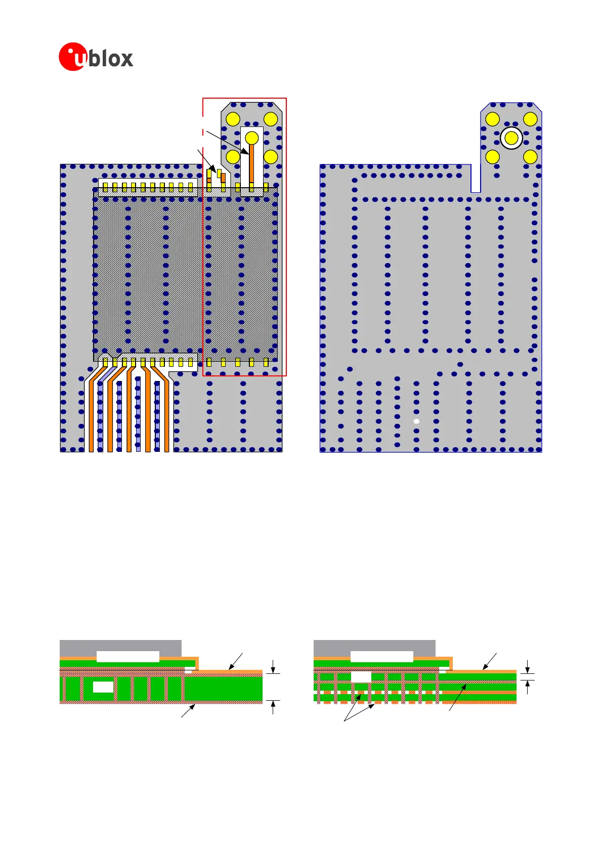
Asseen inFigure 43,anisolatedground areaiscreated aroundandbelowtheRFconnection.This partof the
potentialnoisesourcesaspossible.Makesurethatnosignallinescrossor
a
B and a 4 Layer PCB. The reference ground
Figure 43: Recommended layout for TIM-xx
circuithastobekeptasfarawayfrom
viasofsignaltracesshowupatthePCB
surfaceunderneaththeareasurroundedbytheredrectangle.Also,the
groundplaneshouldbefree fromdigitalsupply returncurrentsinthisarea.Onamultilayerboard,the whole
layer stack below the RF connection should be free of digital lines. This is because even a solid ground
plane
providesonlylimitedisol tion.
Theimpedanceof theantennaconnectionhastomatchthe50Ohmimpedanceof thereceiver.Toachievean
impedanceof50Ohms,thewidthWofthemicrostriphastobechosendependingonthedielectricthickness
H, the dielectric constant ε
r
of the dielectric material of the PCB and on the build-up of the PCB (see
Section 3.6.5). Figure 44 shows two different builds: A 2 Layer PC
planeisinbothdesignsonlayer2(red).Thereforetheeffectivethicknessofthedielectricis
different.
GPS Module
micro strip line
Ground plane
GPS Module
micro strip line
Ground plane
PCB
PCB
Either don't use these layers or fill with ground planes
H
H
Figure 44: PCB build-up for Micro strip line. Left: 2-layer PCB, right: 4-layer PCB
GPSModules-SystemIntegrationManual(SIM)(incl.ReferenceDesign) Design-In
GPS.G4-MS4-05007-A1
Page 55
 Loading...