Zynq-7000 PCB Design Guide www.xilinx.com 55
UG933 (v1.8) November 7, 2014
Chapter 5: Processing System (PS) Power and Signaling
MIO[7] and MIO[8] are dual use pins that are shared with the high-speed
QSPI/NAND/SRAM interface signals. Special care needs to be taken to avoid signal integrity
issues.
CAUTION! If the MIO bank voltage is incorrectly set, the I/O behaves unpredictably and damage might
occur. For example, avoid setting the MIO voltage to 3.3V while using HSTL18. Any pull-up resistors
should only connect to V
CCO_MIO0
.
PS_MIO_VREF – RGMII Reference Voltage
PS_MIO_VREF provides a reference voltage for the RGMII input receivers. If RGMII is being
used, this pin should be tied to a voltage equal to one half V
CCO_MIO1
. For example, when
using a HSTL18 RGMII interface, V
CCO_MIO1
is set to 1.8V then PS_MIO_VREF shall be set to
be 0.9V. A resistor divider can be used to generate PS_MIO_REF. A 0.01 µF capacitor shall be
added for decoupling. If RGMII is not being used, PS_MIO_VREF is safe to float.
Power Sequencing
Refer to DS187, Zynq-7000 All Programmable SoC (Z-7010, Z-7015, and Z-7020): DC and AC
Switching Characteristics and DS191
, Zynq-7000 All Programmable SoC (Z-7030, Z-7045,
and Z-7100): DC and AC Switching Characteristics for power supply sequencing
requirements.
Power Supply Ramp Requirements
Refer to DS187, Zynq-7000 All Programmable SoC (Z-7010, Z-7015, and Z-7020): DC and AC
Switching Characteristics and DS191
, Zynq-7000 All Programmable SoC (Z-7030, Z-7045,
and Z-7100): DC and AC Switching Characteristics for power supply ramp requirements.
PCB Decoupling Capacitors
Decoupling guidelines for the PS supplies can be found in Table 3 - 2 , page 14 .
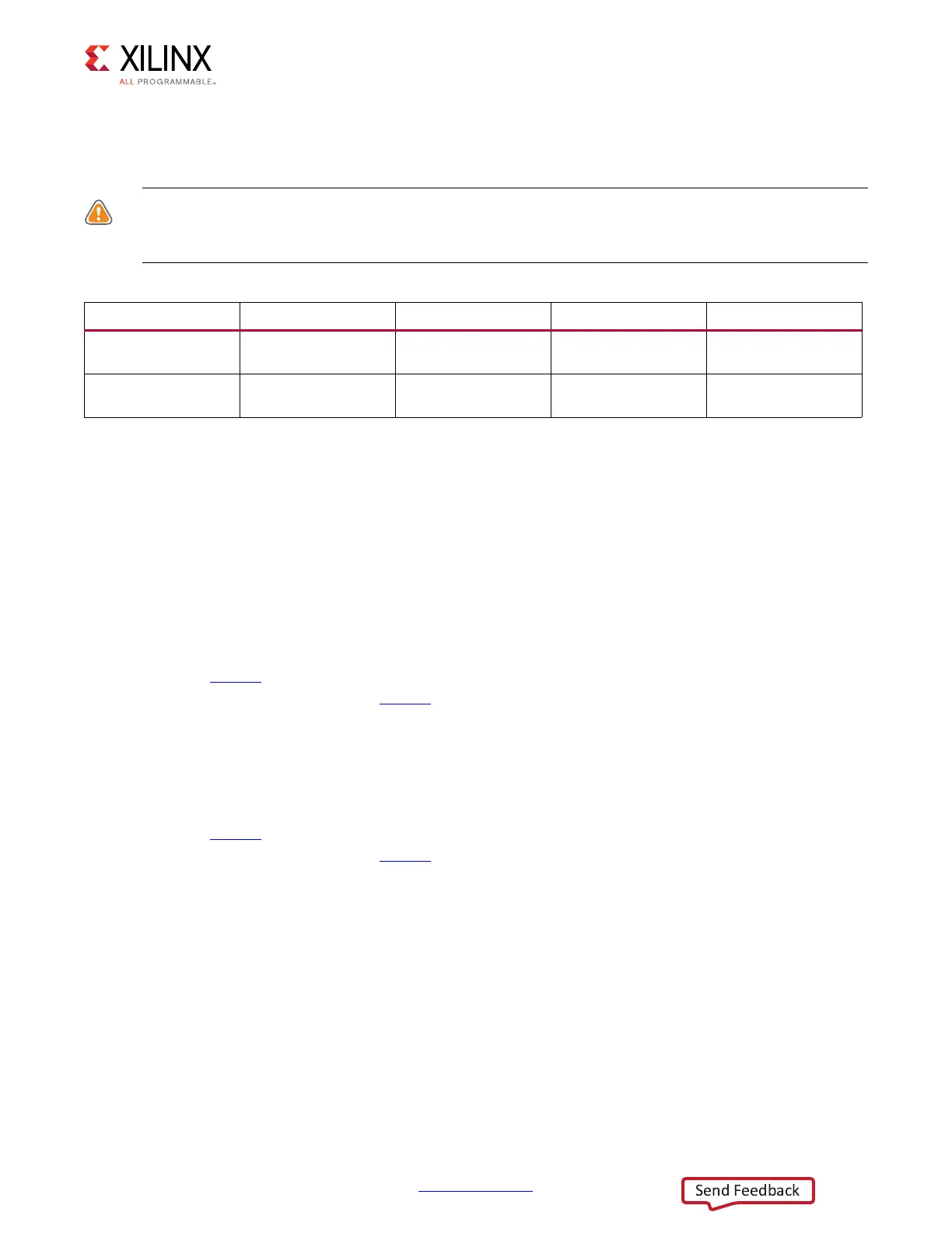
Table 5-3: Voltage Mode Configuration
I/O Bank I/O Supply Name Programming Pin 1.8V Mode 2.5V, 3.3V Modes
MIO Bank 0 V
CCO_MIO0
MIO[7]
20 KΩ resistor to
V
CCO_MIO0
20 KΩ resistor to
ground
MIO Bank 1 V
CCO_MIO1
MIO[8]
20 KΩ resistor to
V
CCO_MIO0
20 KΩ resistor to
ground
 Loading...


