Zynq-7000 PCB Design Guide www.xilinx.com 53
UG933 (v1.8) November 7, 2014
Chapter 5: Processing System (PS) Power and Signaling
PS DDR Power Supplies
V
CCO_DDR
– PS DDR I/O Supply
V
CCO_DDR
is a 1.2V–1.8V nominal supply that supplies the DDR I/O bank input and output
drivers. This supply sources the DDR output drivers, input receivers and termination
circuitry. Its requirements are defined by the type of interface (DDR2, DDR3/3L or LPDDR2),
memory speed, and the data bus width. Table 5-1 shows the supply voltages for the
different memory types.
PS_DDR_VREF0, PS_DDR_VREF1 – PS DDR Reference Voltage
PS_DDR_VREF0 and PS_DDR_VREF1 provide a voltage reference for the PS_DDR_DQ and
PS_DDR_DQS input receivers. They need to be tied to a termination voltage (V
tt
) equal to
V
CCO_DDR
/2. For example, for DDR3, V
CCO_DDR
is set to 1.5V, then V
REF
shall be set to 0.75V.
A resistor divider can be used to generate PS_DDR_VREF0 and PS_DDR_VREF1. A 0.01 µF –
0.47 µF capacitor shall be added for decoupling. The PS DDR reference voltage can also be
generated internally. For LPDDR2, PS_DDR_VREF0/1 shall be set to VDDq/2 in accordance
with the HSUL_12 I/O standard. See section 2.5.7 (MIO Pin Electrical Parameters) in UG585
,
Zynq-7000 All Programmable SoC Technical Reference Manual.
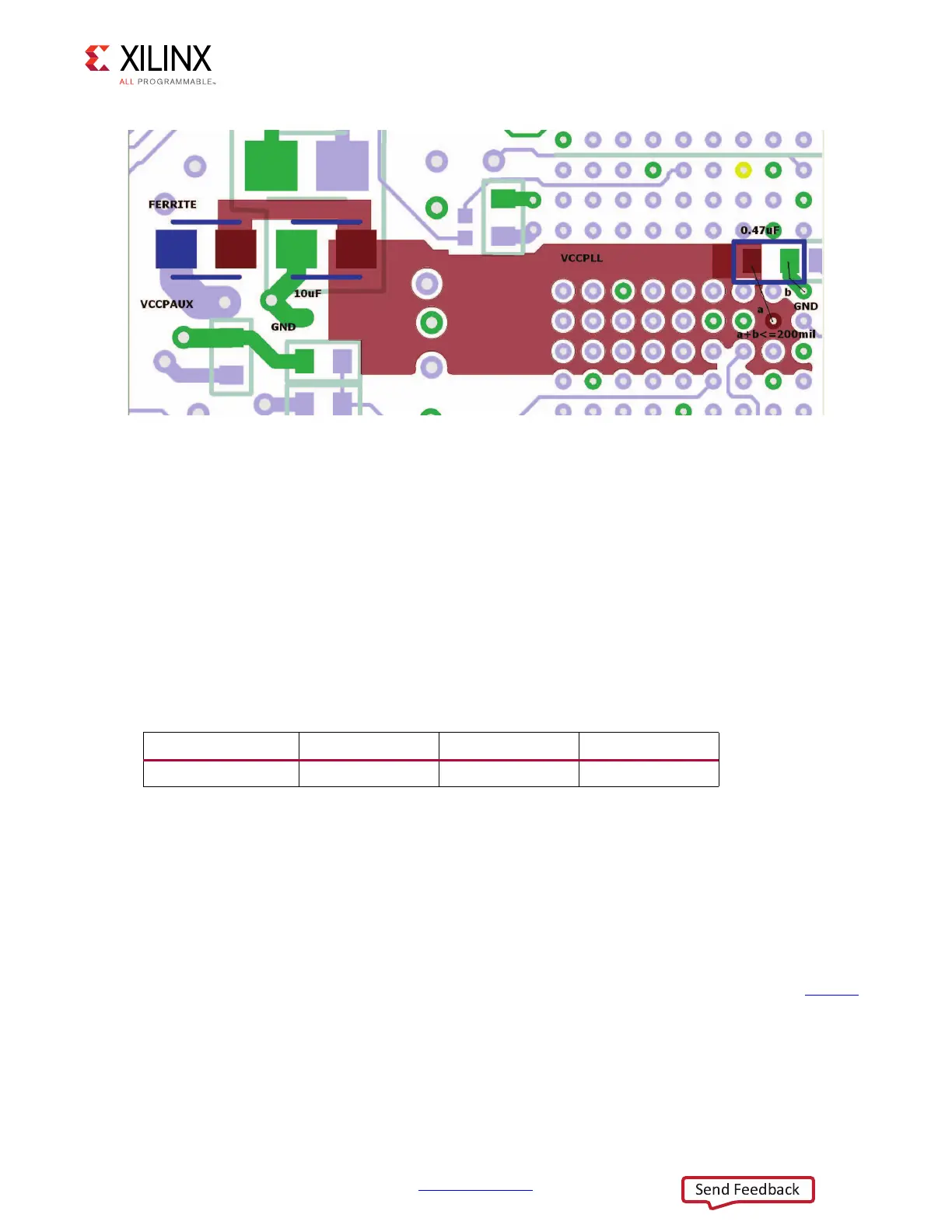
X-Ref Target - Figure 5-3
Figure 5-3: Filtering Circuit Layout
UG933_c5_10_020713
Table 5-1: PS DDR Interface I/O Supply
DDR interface DDR2 DDR3/3L LPDDR2
Voltage 1.8V 1.5V/1.35V 1.2V
 Loading...


