Zynq-7000 PCB Design Guide www.xilinx.com 13
UG933 (v1.8) November 7, 2014
Chapter 3: Power Distribution System
the quantity per I/O bank. Device performance at full utilization is equivalent across all
devices when using these recommended networks.
Table 3-1 and Table 3-2 do not provide the decoupling networks required for the GTX and
GTP transceiver power supplies. For this information, refer to UG476
, 7 Series FPGAs
GTX/GTH Transceivers User Guide and UG482
, 7 Series FPGAs GTP Transceivers User Guide.
RECOMMENDED: Refer to XMP277, 7 Series Schematic Review Recommendations, for a comprehensive
checklist for schematic review which complements this document.
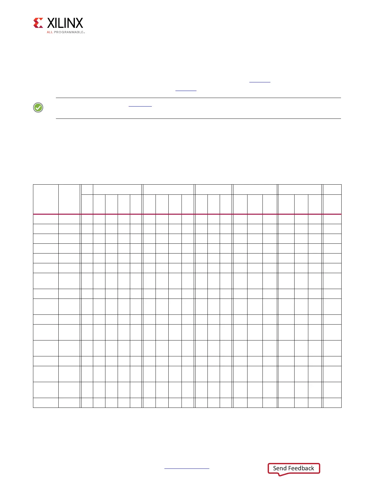
Required PCB Capacitor Quantities
Table 3-1 lists the PCB decoupling capacitor guidelines per V
CC
supply rail for Zynq-7000 AP
SoC devices.
Table 3-1: Required PCB Capacitor Quantities per Device (PL)
Package Device
V
CCINT
V
CCBRAM
V
CCAUX
V
CCAUX_IO
V
CCO
per Bank
(3)(4)
Bank 0
680
µF
330
µF
100
µF
4.7
µF
0.47
µF
100
µF
47
µF
4.7
µF
0.47
µF
47
µF
4.7
µF
0.47
µF
47
µF
4.7
µF
0.47
µF
47 µF
or
100 µF
4.7
µF
0.47
µF
47
µF
CLG225 Z-7010 0 0 1 1 2 NA NA NA NA 1 1 1 NA NA NA 1 2 4 1
CLG400 Z-7010 0 0 1 1 2 0 1 1 1 1 1 1 NA NA NA 1 2 4 1
CLG485 Z-7015 0 1 0 2 4 1 0 1 1 1 1 2 NA NA NA 1 2 4 1
CLG400 Z-7020 0 1 0 2 4 1 0 1 1 1 1 1 NA NA NA 1 2 4 1
CLG484 Z-7020 0 1 0 2 4 1 0 1 1 1 1 2 NA NA NA 1 2 4 1
SBG485 Z-7030 0 1 0 1 0 1 0 1 2 1 0 0 NA NA NA 1 0 0 1
FBG484/
RB484
Z-703001010101 2 100NANANA 1 0 0 1
FBG676 Z-7030 0 1 0 1 0 1 0 1 2 1 0 0 1 0 0 1 0 0 1
FFG676/
RF676
Z-703001010101 2 100 1 0 0 1 0 0 1
FBG676 Z-7035 2 0 0 2 1 0 2 4 1 0 0 1 0 0 1 0 0 1 1
FFG676/
RF676
Z-703520021024 1 001 0 0 1 0 0 1 1
FFG900/
RF900
Z-703520011024 1 001 0 0 1 0 0 1 1
FBG676 Z-7045 2 0 0 2 0 1 0 2 4 1 0 0 1 0 0 1 0 0 1
FFG676/
RF676
Z-704520020102 4 100 1 0 0 1 0 0 1
FFG900/
RF900
Z-7045
20010102 4 100 1 0 0 1 0 0 1
FFG900 Z-7100 3 0 0 2 0 2 0 4 8 1 0 0 1 0 0 1 0 0 1
 Loading...


