Zynq-7000 PCB Design Guide www.xilinx.com 70
UG933 (v1.8) November 7, 2014
Chapter 6: Migration from XC7Z030-SBG485 to XC7Z015-CLG485 Devices
Functional and Performance Differences
The main functional and performance-related difference between the two devices is the
programmable logic upon which each is based. The XC7Z030-SBG485 device utilizes
Kintex®-7 logic, the XC7Z015-CLG485 device utilizes Artix®-7 logic. Kintex-7 device
performance characteristics are higher than Artix-7 device performance characteristics, as
Artix-7 devices are generally geared for lower-cost applications. There will be timing
differences as a result, so careful timing analysis will need to be performed. For a general
overview of Zynq-7000 devices as they pertain to Kintex-7 and Artix-7 device architectures,
refer to the Zynq-7000 All Programmable SoC Overview (DS190
). For more specific
information regarding Kintex-7 and Artix-7 device architectures, refer to the Kintex-7 FPGAs
Data Sheet (DS182
), and the Artix-7 FPGAs Data Sheet (DS181).
Package Differences
The second-most important difference is in regards to packaging. The different package
types (bare/flip chip versus wirebond) results in flight time differences between same I/Os.
For designs targeting maximum performance, PCB and system simulations are crucial to
determine if system-wide timing can be met.
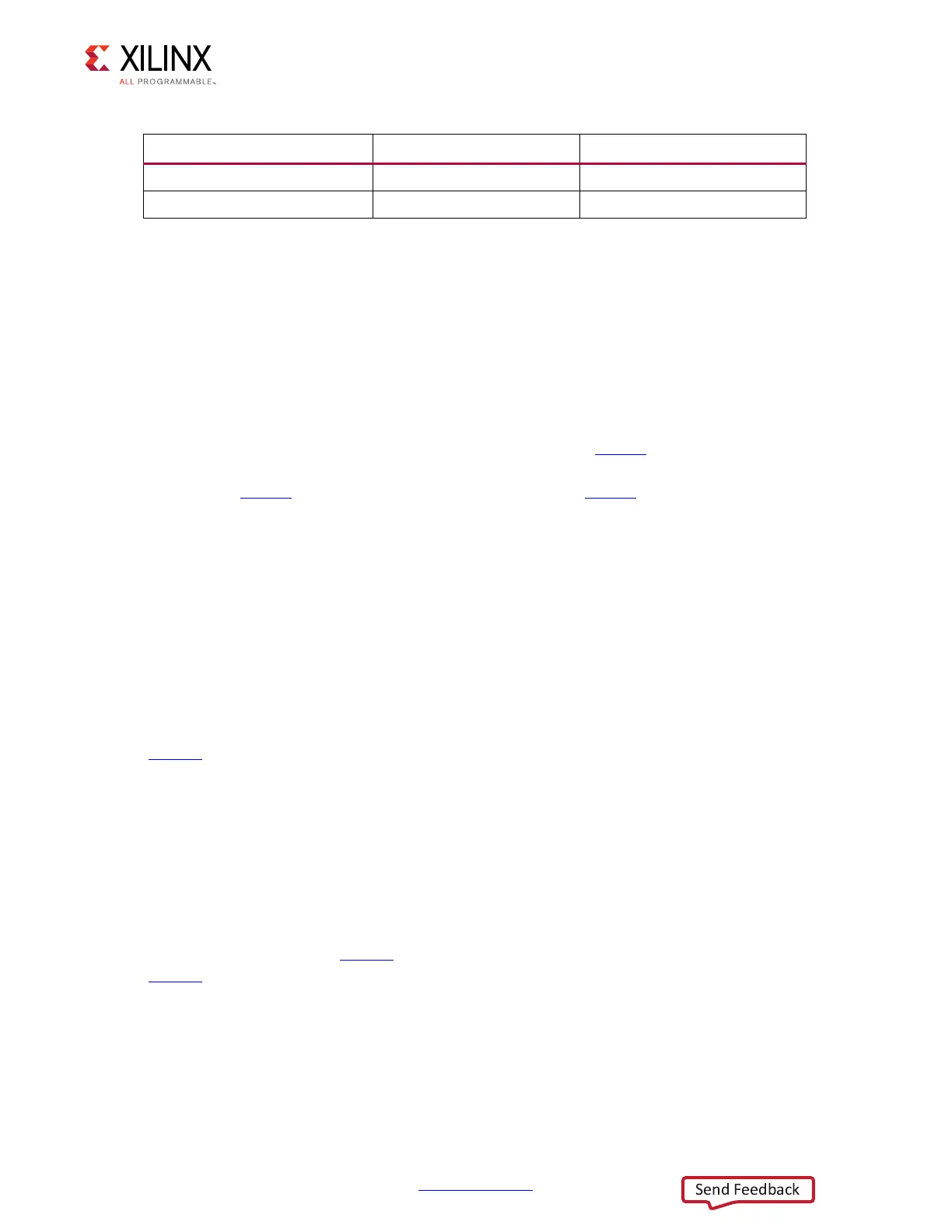
There are also a number of pinout differences between the two packages, as noted in
Table 6-1. Full package details, including links to the respective package files, can be found
in the Zynq-7000 All Programmable SoC Packaging and Pinout Product Specification
(UG865
).
Transceiver Differences
The XC7Z030-SBG485 device utilizes the higher-performance GTX transceivers, the
XC7Z015-CLG485 device utilizes high performance GTP transceivers. GTX and GTP
transceivers share many of the same features, but some notable differences are in regards
to power supply tolerances, as well as different transceiver software wizards. For more
information about GTX and GTP transceivers, please refer to the 7 Series FPGAs GTX/GTH
Transceiver s User Guide (UG476
), as well as the 7 Series FPGAs GTP Transceivers User Guide
(UG482
).
PCB Layout Considerations
The key items to note from a PCB layout perspective are that banks 34 and 35 are high
performance I/O banks in the XC7Z030-SBG485 device, so care must be made not to exceed
valid voltage levels on those banks. In addition, bank 112 contains two pins that are not
Bank 112, pin W3 MGTVCCAUX Not Connected
Xilinx Design Software Vivado and ISE Vivado Only
Table 6-1: Key Differences Between XC7Z030-SBG485 and XC7Z015-CLG485 Devices (Cont’d)
XC7Z030-SBG485 XC7Z015-CLG485
 Loading...


