Zynq-7000 PCB Design Guide www.xilinx.com 63
UG933 (v1.8) November 7, 2014
Chapter 5: Processing System (PS) Power and Signaling
In addition, DDR signals also require matched trace delays, which include package delays.
Table 5-9 shows the recommended delay matching for DDR. Differential traces should be
delay matched such that the signal crossing point occurs in the linear region of the rising
and falling edges.
The skew limits can be increased if the memory interface is not operated at the maximum
frequency, and/or if a faster memory device is utilized. If running a DDR2 interface at
800 MHz, using a 1,066 MHz memory relaxes the skew from 20 pS to 82 pS. If running a
DDR3 interface at 1,066 MHz, using a 1,333 MHz memory device relaxes the skew from
10 pS to 45 pS.
To ensure proper write leveling for DQS to clock delays, route the CK trace to be equal to or
longer than the DQS trace per byte lane.
DDR Trace Impedance
All DDR signals except DDR_DRST_B require controlled impedance. DDR_CKE also requires
controlled impedance in DDR3/3L. Table 5-10 shows the required trace impedance for DDR
signals.
DDR3 and LPDDR2 memory also require an additional resistor connected to the ZQ pin to
calibrate the device's output impedance. Table 5-11 shows the required RZQ values.
Ω
DDR Routing Topology
Based on the chosen memory type, the number of memory devices and layout
requirements, different routing topologies can be used for DDR memory. Figure 5-8 shows
two different topologies.
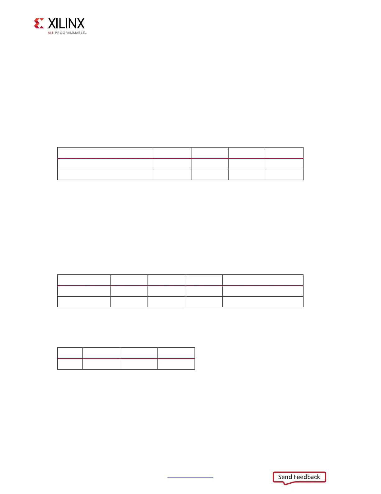
Table 5-9: DDR Delay Match
Signal Group LPDDR2 DDR2 DDR3/3L Comments
DQ/DM to DQS_P/N in data group ±10 ps ±20 ps ±10 ps
Address/Control to CK_P/N ±10 ps ±25 ps ±10 ps
Table 5-10: DDR Trace Impedance
Signal Group LPDDR2 DDR2 DDR3/3L Comments
Single-ended 40Ω 50Ω 40Ω ±10% tolerance
Differential 80
Ω 100Ω 80Ω ±10% tolerance
Table 5-11: DDR ZQ
ZQ LPDDR2 DDR2 DDR3/3L
Rzq 240Ω N/A 240Ω
 Loading...


