Zynq-7000 PCB Design Guide www.xilinx.com 69
UG933 (v1.8) November 7, 2014
Chapter 6
Migration from XC7Z030-SBG485 to
XC7Z015-CLG485 Devices
Introduction
Package migration across a device family is a common feature among Xilinx devices. The
pinout remains consistent, with the biggest difference being more available I/Os in bigger
packages. However, a unique case arises when migrating from an XC7Z030-SBG485 device
to an XC7Z015-CLG485 device, as there are more significant differences between the
devices other than pinout. The designer wishing to migrate between these two devices
needs to be aware of these differences.
Differences between XC7Z030-SBG485 and
XC7Z015-CLG485 Devices
When migrating from an XC7Z030-SBG485 device to an XC7Z015-CLG485 device, some key
differences should be noted in regards to functionality, performance, packaging,
transceivers, PCB layout, and software (see Table 6-1).
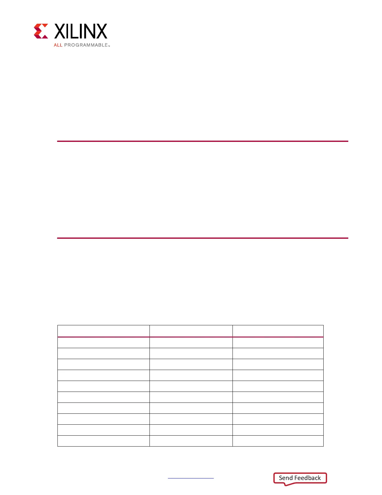
Table 6-1: Key Differences Between XC7Z030-SBG485 and XC7Z015-CLG485 Devices
XC7Z030-SBG485 XC7Z015-CLG485
Die/Fabric Kintex-7 Artix-7
Package Type Bare/Flip Chip Wirebond
Processor Speed 1 GHz 800 MHz
Power Supply Tolerance 3% 5%
Bank 34, pins H8/R8 VRP/VRN (for DCI) No DCI
Bank 35, pins H5/H6 VRP/VRN (for DCI) No DCI
Bank 34 HP I/Os HR I/Os
Bank 35 HP I/Os HR I/Os
Bank 112 (MGT) GTX GTP
Bank 112, pin V7 MGTAVTTRCAL Not connected
 Loading...


