Zynq-7000 PCB Design Guide www.xilinx.com 54
UG933 (v1.8) November 7, 2014
Chapter 5: Processing System (PS) Power and Signaling
PS_DDR_VRN, PS_DDR_VRP – PS DDR Termination Voltage
PS_DDR_VRN and PS_DDR_VRP provide a reference for digitally controlled impedance (DCI)
calibration. For memory types that require termination (DDR2, DDR3) VRP must be pulled
Low to GND and VRN needs to be pulled High to V
CCO_DDR
. For DDR2/3, the resistor value
on VRP and VRN should be twice the memory's trace and termination impedance. For
example, for a DDR3 memory with a 40Ω termination and board impedance, an 80Ω resistor
must be used to pull-up/down VRP and VRN. For LPDDR2, the DCI tunes the output
impedance of the driver and therefore the resistor value on VRP and VRN should be equal
to the transmission line impedance, typically set to 40Ω.
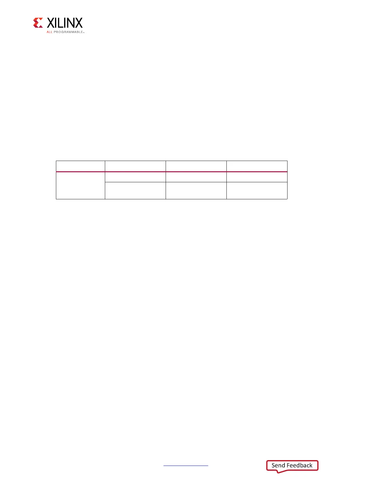
Table 5-2 shows the required values for the DCI VRN/VRP pull-down/pull-up resistors.
Unused DDR Memory
When no PS DDR memory is used, V
CCO_DDR
should be tied to V
CCPAUX
. PS_DDR_VREF0/1
and PS_DDR_VRN/P should be left floating.
PS MIO Power Supplies
V
CCO_MIO0
– PS MIO Bank 0 I/O Supply
V
CCO_MIO0
is a 1.8–3.3 volt supply. It powers I/O Bank 500 which contains PS_MIO[15:0],
PS_CLK, and PS_POR_B I/Os.
V
CCO_MIO1
– PS MIO Bank 1 I/O Supply
V
CCO_MIO1
is a 1.8-3.3 volt supply. It powers I/O Bank 501 which contains PS_MIO[53:16],
PS_VREF_MIO, and PS_SRST_B I/Os.
Configuring the V
CCO_MIO0
, V
CCO_MIO1
Voltage Mode
The PS I/O banks can operate in two different voltage modes, low (1.8V) mode and high
(2.5V – 3.3V) mode. Before powering on, the banks must be configured for the correct mode
otherwise, damage might occur. The I/O bank voltage is set by pulling pins MIO[7] and
MIO[8] either High or Low. Table 5-3 shows the voltage mode configuration (VMODE) for
MIO Bank 0 and Bank 1.
Table 5-2: DCI VRP and VRN Values
LPDDR2 DDR2 DDR3/3L
VRP/VRN
40Ω 100Ω 80Ω
(type I DCI trace
impedance 40
Ω)
(type III DCI trace
impedance 50Ω)
(type III DCI trace
impedance 40Ω)
 Loading...


