UG-570 AD9361 Reference Manual
| Page 118 of 128
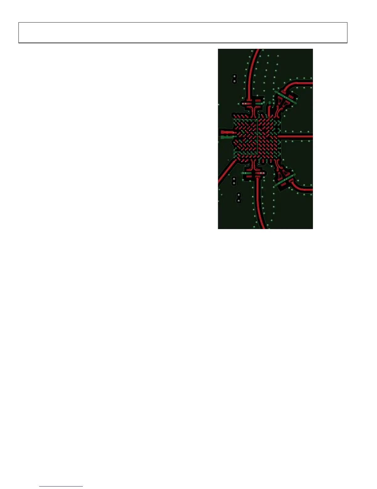
RF TRANSMISSION LINE LAYOUT
The AD9361 evaluation boards use micro strip lines for all the
RF traces. The critical Rx and Tx lines route on the top side of
the board. It is not recommend to use vias to route RF traces.
The differential lines from the balun secondary to the Rx and
Tx balls need to be as short as possible. The length of the single-
ended transmission line should be short to minimize the effects
of parasitic coupling. Since the receiver front end is DC-biased
internally, the differential side of the balun is ac-coupled. The
system designer can optimize the RF performance with a proper
selection of the balun and the ac-coupling capacitors. The Tx
monitor traces, external LO traces and the external clock traces
could require matching components as well, to ensure best
performance.
All the previous RF signals mentioned must have a solid ground
reference under them. None of the critical traces should run
over a section of the reference plane that is discontinuous. The
ground flood on the reference layer must extend all the way to
the edge of the board. This ensures good signal integrity for the
SMA launch.
See the RF Port Interface section for more information on the
RF matching issues associated with the AD9361.
Figure 86. RF Match Structures on Rx and Tx on FMComms2 Board

 Loading...


