AD9361 Reference Manual UG-570
| Page 101 of 128
The data samples are carried in two’s complement format, with
D[11] as the numerically most significant bit and D[0] as the
least significant bit. The most positive sample value is 0x7FF
and the most negative value is 0x800. For a single RF path in
each direction (that is, a 1R1T system), the I and Q samples are
separated with I data on P0_D[11:0] and Q data on P1_D[11:0]
as follows:
P0: I, I, I, …
P1: Q, Q, Q, …
For a system with two active Rx channels, the I and Q samples
from RF Path 1 and RF Path 2 are carried in a 2-way interleave
with I samples on P0 and Q samples on P1.
P0: I
1
, I
2
, I
1
, I
2
, …
P1: Q
1
, Q
2
, Q
1
, Q
2
, …
For a system with a 2R1T or a 1R2T configuration, the clock
frequencies, sample periods, and data capture timing are the
same as if configured for a 2R2T system. However, in the path
with only a single channel used, the disabled channel’s I-Q pair
in each data group is unused. As an example, for a 2R1T system
with only the Tx Channel 1 used, the Tx burst would have two
unused slots, as follows:
The AD9361 captures P0: I
1
, X, I
1
, X , …
P1: Q
1
, X, Q
1
, X , …
The unused X slots can be filled with arbitrary data values by
the BBP. Such values can be either constant values, or the
preceding data sample values can be repeated to reduce the bus
switching factor and, therefore, power consumption.
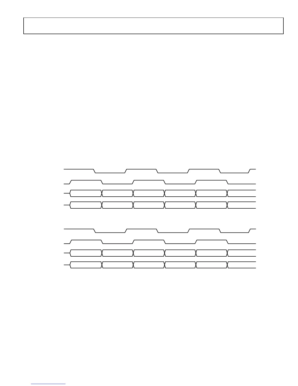
DUAL PORT TDD FUNCTIONAL TIMING (CMOS)
The timing diagrams in Figure 71 and Figure 72 illustrate the
relationship among the bus signals in dual port TDD mode.
Note that because 2R1T and 1R2T systems follow the 2R2T
timing diagrams, they are omitted from these Figure 71 and
Figure 72.
Figure 71
. Receiver Data Path, Dual Port TDD
DATA _CLK
RX_FRAME
P0_D[11:0]
P1_D[11:0]
1R1T, DDR, TDD, DUAL PORT, 0x010 = 0xC8, 0x011 = 0x00, 0x012 = 0x08
R1_I[11:0] R1_I[11:0] R1_I[11:0] R1_I[11:0] R1_I[11:0] R1_I[11:0]
R1_Q[11:0] R1_Q[11:0] R1_Q[11:0] R1_Q[11:0] R1_Q[11:0] R1_Q[11:0]
11668-073
DATA _CLK
RX_FRAME
P0_D[11:0]
P1_D[11:0]
2R2T, DDR, TDD, DUAL PORT, 0x010 = 0xC8, 0x011 = 0x00, 0x012 = 0x08
R1_I[11:0] R2_I[11:0] R1_I[11:0] R2_I[11:0] R1_I[11:0] R2_I[11:0]
R1_Q[11:0] R2_Q[11:0] R1_Q[11:0] R2_Q[11:0] R1_Q[11:0] R2_Q[11:0]

 Loading...


