UG-570 AD9361 Reference Manual
| Page 16 of 128
RF AND BBPLL SYNTHESIZER
OVERVIEW
The AD9361 transceiver contains two identical RFPLL
synthesizers to generate the required LO signals, which are
programmed independently. One is programmed for the Rx
channel and the other for the Tx channel. The transceiver also
contains a BBPLL synthesizer to generate the required sampling
and internal operational clocks. The PLL synthesizers are all of
fractional–N architecture with completely integrated VCOs and
loop filters. They require no external parts to cover the entire
frequency range of the device. This configuration allows the use
of any convenient reference frequency for operation on any
channel with any sample rate. For FDD operation, the
frequency of Tx and Rx can be the same or different, and both
RFPLL synthesizers operate simultaneously. For TDD
operation, the RFPLL synthesizers alternately turn on as
appropriate for Rx and Tx frames.
RFPLL INTRODUCTION
The fundamental frequency of the RFPLLs is from 6 GHz to
12 GHz. Local oscillator frequencies ranging from 47 MHz to
6 GHz are created by dividing the PLL frequency. The Rx PLL is
configured and calibrated using the ad9361_set_rx_lo_freq
function, and the Tx PLL is configured using the
ad9361_set_tx_lo_freq function. Each synthesizer must be
configured and calibrated separately.
AD9361 PLL ARCHITECTURE
The following sections show block diagrams of the AD9361 PLL
that consist of the reference block, the main PLL block, and the
LO GEN output block. The VCO always operates between
6 GHz to 12 GHz.
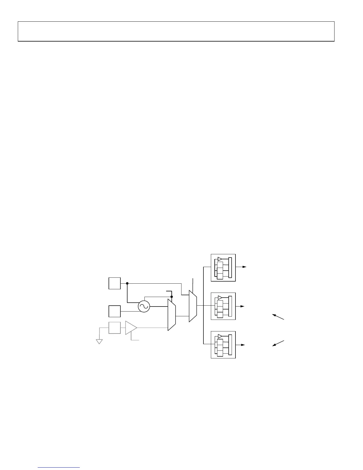
REFERENCE BLOCK
The reference frequency can be generated via the on-chip
DCXO or an external clock source can provide this input to the
device. A MUX selects the desired source. The reference is then
split and applied to three independent conditioning blocks also
known as ref dividers. The conditioning blocks provide four
options such that the PLL reference frequency, F
REF
, (the loop
reference applied to the PLL phase detector) is either buffered,
doubled, halved, or divided by 4. Independent blocks make it
possible to have a different F
REF
for the RF and BBPLLs. The
reference scalers will be set by the ad9361_init function. For
best RFPLL performance, Analog Devices recommends
selecting a reference clock or crystal that will be able to scale as
close to 80 MHz as possible.
Figure 3.
PLL Reference Block
H6
DO NOT USE
CONNECT H6 TO GROUND
DCXO
20MHz TO 50MHz
M11
M12
1
0
1
0
BBPLL
F
REF
FOR BEST
PERFORMANCE:
35MHz TO 80MHz
FOR BEST
PERFORMANCE:
35MHz TO 70MHz
XTALP OR
OPEN FOR EXTERNAL REFERENCE
XTALN OR
EXTERNAL REFERENCE INPUT
5MHz TO 320MHz
(19MHz TO 80MHz RECOMMENDED)
÷2
÷4
×2
÷2
÷4
×2
÷2
÷4
×2
TX SYNTH
F
REF
RX SYNTH
F
REF
10MHz TO 80MHz
10MHz TO 80MHz
11668-004

 Loading...


