AD9361 Reference Manual UG-570
| Page 69 of 128
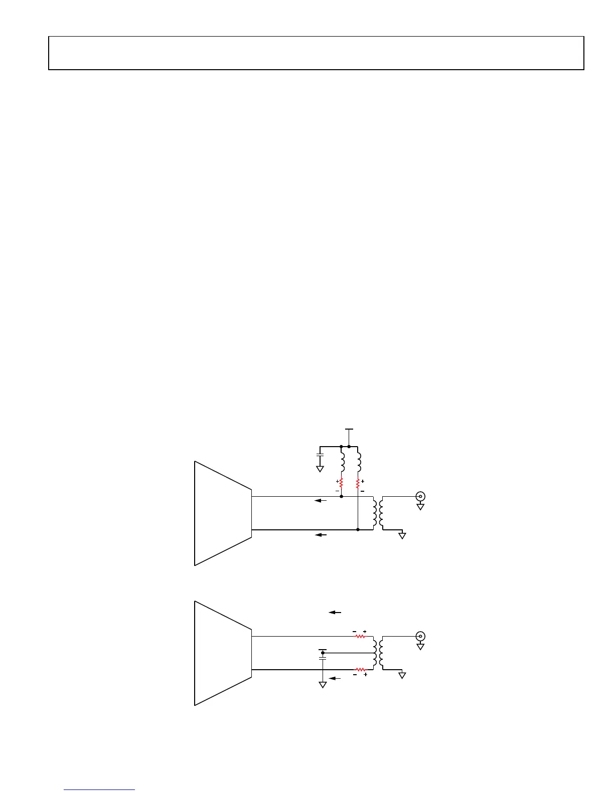
Tx SIGNAL PATH INTERFACE
The AD9361 transmit path covers a full 70 MHz to 6.0 GHz
transmit frequency range and the 2 Tx outputs exhibit similar
performance. The Tx outputs are differential and require an
external output bias. These outputs need to be biased to 1.3 V
DC supply voltage (nominal) using either chokes (wire-wound
inductors) or a transformer center tap connection. Each side of
the differential output draws ≈75 mA of DC bias current at full
output power. It is important to select components with low DC
resistance (R
DCR
) to minimize voltage drop ΔV across the series
parasitic resistance element (see the red resistor symbol in
Figure 49). As the ΔV voltage drop increases, the Tx buffer RF
performance (OP1dB, max output power) degrades. Choke
inductance (L
C
) should be selected such that the choke
impedance is high enough relative to the load impedance so
that it does not affect the frequency response. The Tx outputs
will have to be ac-coupled in most applications due to the
presence of 1.3 V DC supply bias voltage. The approach in
Figure 50 is preferred because there are fewer parasitics and the
component count is lower.
The Tx differential output port is a medium signal device.
Therefore, impedance matching is based on load-pull
techniques. Very similar to a PA (power amplifier). The goal is
to provide a Tx output differential load impedance that
represents the best compromise between the maximum output
power delivered and the highest possible third-order linearity
(OIP3).
Load-pull based impedance matching is very simple. The focus
is on developing the preferred load impedance at the Tx output
ball pads. This matching technique is quite different from the
small-signal techniques utilized for the Rx input.
• Load-pull: Design the matching network for the preferred
Load impedance at the Tx output pads.
• Small-signal: Design the matching network for maximum
power transfer (TG: transducer gain).
Based on present load-pull data, the preferred Tx output
differential load impedance is 50 Ω.
• The reference plane is the Tx output ball pads.
• The fundamental power is inversely proportional to the
real part of the load impedance.
• The OIP3 is inversely proportional to the real part of the
load impedance.
• The OIP3 is higher for capacitive loads as compared to
inductive loads. If residual impedance matching errors
exist, it is better to error with a capacitive termination as
opposed to an Inductive termination.
Figure 51 to Figure 54 show the basic differential Tx output
interface configurations. Note that matching networks (balun
single-ended port) will most likely be required to achieve
optimum performance.
Figure 49. AD9361 Tx Output DC Biasing Using Chokes
Figure 50. AD9361 Tx Output DC Biasing Using Center Tapped Transformer
1.3V
TXA_N
TXA_P
TX OUTPUT
C
B
L
C
L
C
R
DCR
R
DCR
1.3V – ΔV
1.3V – ΔV
ΔV ΔV
I
BIAS
~75mA
I
BIAS
~75mA
11668-050
TXA_N
TXA_P
TX OUTPUT
I
BIAS
~75mA
I
BIAS
~75mA
1.3V
ΔV
ΔV
1.3V – ΔV
1.3V – ΔV
C
B
11668-051

 Loading...


